Semiconductor material energy gap measuring method and device

A measurement method and technology of a measurement device, which are applied in the direction of material analysis using measurement of secondary emissions, and can solve problems such as the decline of measurement accuracy

Active Publication Date: 2020-05-26
YANGTZE MEMORY TECH CO LTD
View PDF4 Cites 2 Cited by
  • Summary
  • Abstract
  • Description
  • Claims
  • Application Information

AI Technical Summary

Problems solved by technology

However, the measurement signal obtained by this method not only contains energy gap information, but also contains strong plasmon information, which will have a great impact on the energy gap analysis, resulting in a decrease in measurement accuracy.

Method used


Image

  • Semiconductor material energy gap measuring method and device
  • Semiconductor material energy gap measuring method and device
  • Semiconductor material energy gap measuring method and device

Examples


Embodiment Construction

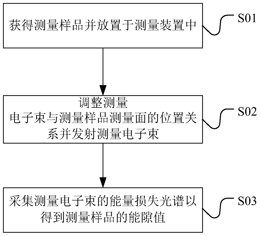
[0025] Hereinafter, the present invention will be described in more detail with reference to the accompanying drawings. In the various figures, identical elements are indicated with similar reference numerals. For the sake of clarity, various parts in the drawings have not been drawn to scale. Also, some well-known parts may not be shown in the drawings.

[0026] In the following, many specific details of the present invention are described, such as device structures, materials, dimensions, processing techniques and techniques, for a clearer understanding of the present invention. However, the invention may be practiced without these specific details, as will be understood by those skilled in the art.

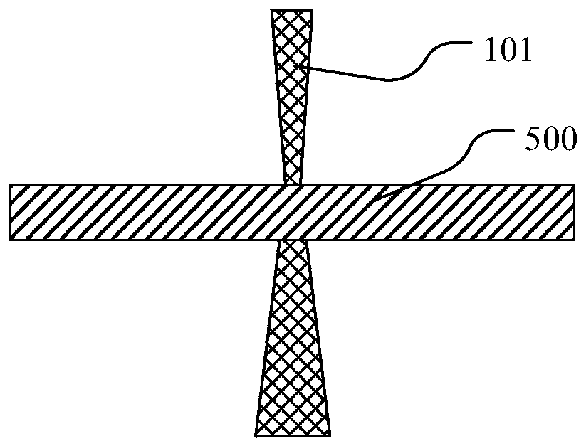
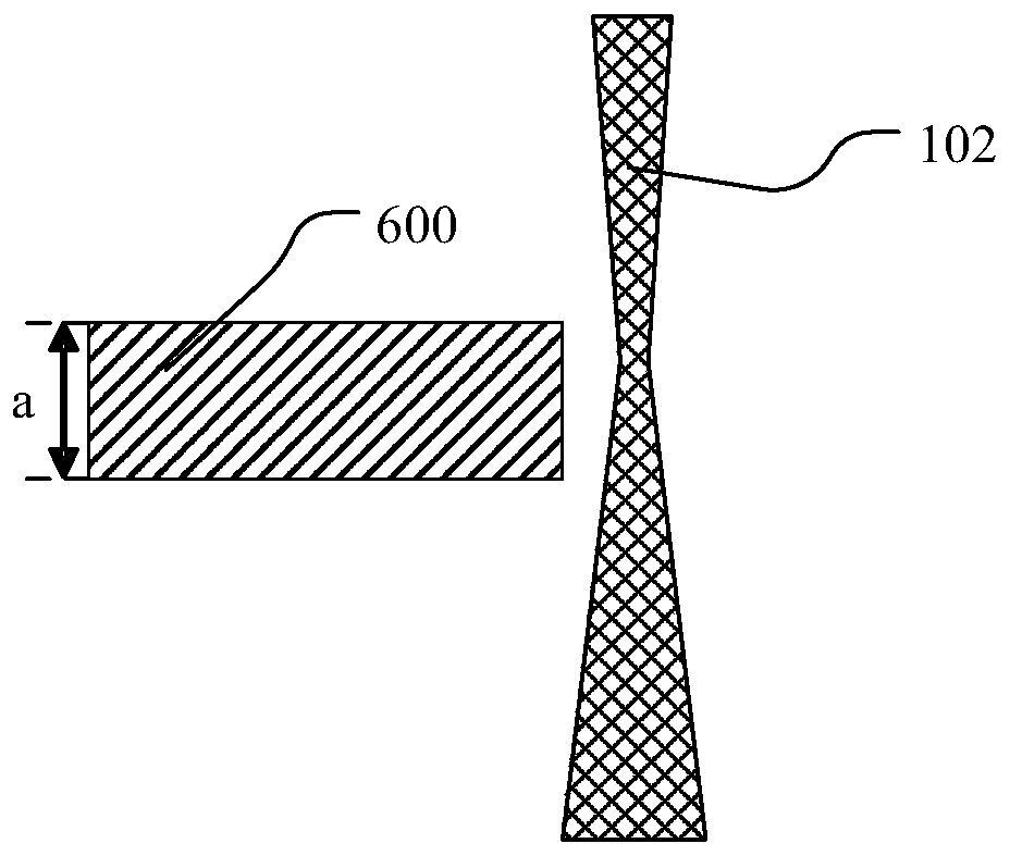
[0027] In this application, the term "energy gap" is also called "band gap", which is used to characterize the energy gap from the top of the valence band to the bottom of the conduction band of a semiconductor or insulator. Among them, the outermost electrons in the atom ar...


PUM


Abstract

The invention provides a semiconductor material energy gap measuring method and device. The measuring method comprises the steps: a measuring sample is obtained and placed in a measuring device; the position relationship between the measurement electron beam and the measurement surface of the measurement sample is adjusted and the measurement electron beam is emitted; and an energy loss spectrum of the measurement electron beam is collected to obtain an energy gap value of the measurement sample, wherein the emitting direction of the measurement electron beam is parallel to the measurement surface of the measurement sample. The measurement electron beam and the measurement surface of the measurement sample are parallel to each other and are not in contact with each other, so that the acquired electron energy loss spectrum is prevented from containing exciton information, and the energy gap measurement accuracy is further improved.

Description

technical field [0001] The invention relates to the technical field of semiconductor measurement, and more specifically, to a method and device for measuring an energy gap of semiconductor materials. Background technique [0002] At present, in order to increase the storage capacity of a storage device, a 3D stacking technology is generally used to achieve high performance and high integration of the storage device. In a highly integrated memory device, the conductivity of the semiconductor material determines the performance of the memory device. At present, in the process of manufacturing 3D memory devices, it is particularly important to perform energy gap engineering on the silicon compound layer and the conductive layer. [0003] The existing technology generally uses electron energy loss spectroscopy to measure the energy gap value of semiconductor materials. This method guides the generated electron beam through the film to be tested and collects the interacting elec...

Claims


Application Information

Patent Timeline
Patent Type & Authority Applications(China)
IPC IPC(8): G01N23/22
CPCG01N23/22
Inventor 李国梁魏强民
Owner YANGTZE MEMORY TECH CO LTD
Why Eureka
Try Eureka