Circuit structure and manufacturing method thereof

A technology of circuit structure and manufacturing method, applied in the direction of circuits, semiconductor/solid-state device parts, nanotechnology for materials and surface science, etc., can solve problems such as peeling and fracture, achieve increased structural strength, simple process steps, The effect of improving product reliability

Active Publication Date: 2021-09-07
WINBOND ELECTRONICS CORP
View PDF0 Cites 0 Cited by
  • Summary
  • Abstract
  • Description
  • Claims
  • Application Information

AI Technical Summary

Problems solved by technology

Therefore, the interface between the traditional redistribution layer structure and the copper pillar bump often suffers from peeling and fracture problems during reliability testing

Method used


Image

  • Circuit structure and manufacturing method thereof
  • Circuit structure and manufacturing method thereof
  • Circuit structure and manufacturing method thereof

Examples


Embodiment Construction

[0011] Order to more fully illustrate the embodiments of the present invention with reference to the drawings. However, the present invention may be embodied in various different forms and should not be limited to the embodiments described herein. FIG. Layer with a thickness in the region of the figures will be exaggerated for clarity. The same or similar reference numerals designate the same elements or similar elements, it will not further described in the following paragraphs.

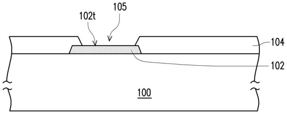
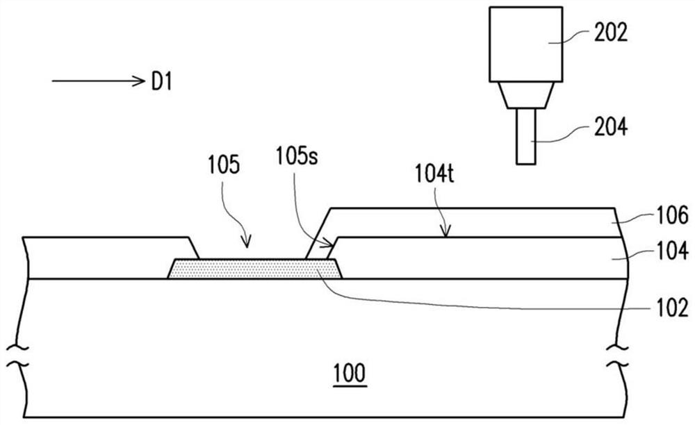
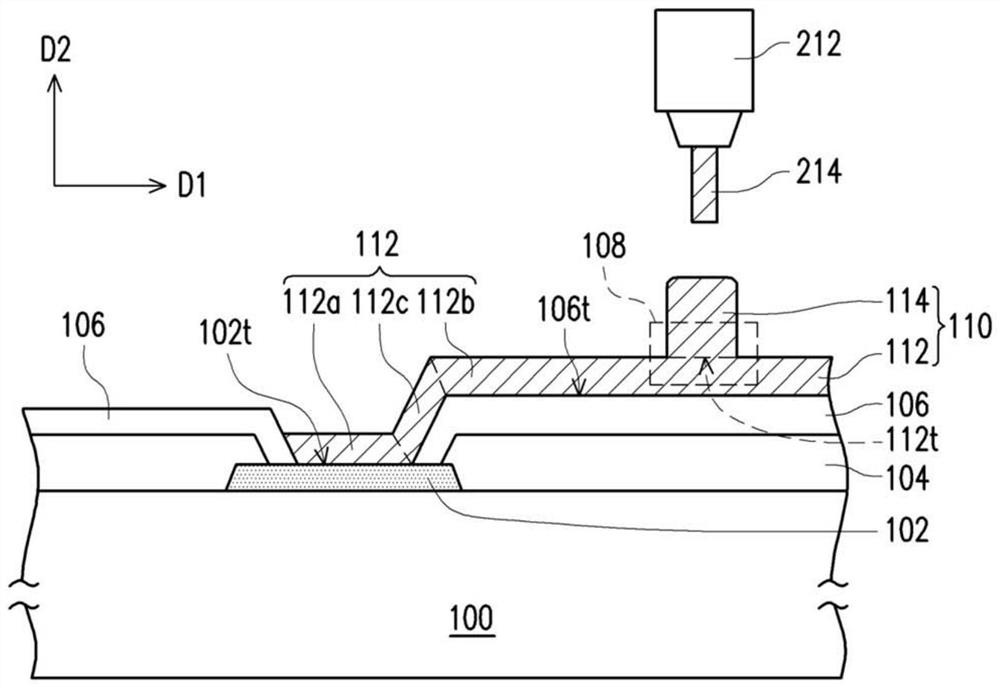
[0012] Figure 1A to 1E It is a schematic diagram cross-sectional manufacturing process a wiring structure according to an embodiment of the present invention. figure 2 Yes Figure 1C A cross-sectional view of a portion of an enlarged view of line structure. Thereto, the present embodiment illustrated embodiment may be a wiring structure redistribution layer (RDL) structure, but the present invention is not limited thereto. In other embodiments, the structure may be a line rear section (back-end-of-line,...


PUM

PropertyMeasurementUnit
thicknessaaaaaaaaaa
thicknessaaaaaaaaaa
particle sizeaaaaaaaaaa

Abstract

The invention provides a circuit structure, including: a base, a pad, a dielectric layer, a conductive layer, an adhesive layer and a conductive bump. The pads are disposed on the substrate. The dielectric layer is disposed on the base and exposes part of the pads. The conductive layer contacts the pad and extends from the pad to cover the top surface of the dielectric layer. The adhesive layer is configured between the dielectric layer and the conductive layer. The conductive bump extends upward from the top surface of the conductive layer. The conductive bump and the conductive layer are integrally formed. In addition, a method for manufacturing the circuit structure is provided.

Description

Technical field [0001] The present invention relates to a semiconductor structure and a manufacturing method, particularly to a circuit structure and manufacturing method. Background technique [0002] In recent years, since the product set of the various electronic components (e.g. transistors, diodes, resistors, capacitors, etc.) continue to improve, and thus the rapid growth of the semiconductor industry. This product set to enhance the degree, mostly because of the minimum feature sizes continue to shrink, so that more integrated member in a particular area. [0003] Compared with the conventional package structure, smaller size of these electronic components having a small area, thus requiring a smaller package structure. For example, semiconductor chip or die with more input / output (I / O) pad, redistribution layer (redistribution layer, RDL) of the semiconductor chip may be raw or die I / O pads re-layout position around the semiconductor chip or die, to increase the I / ...

Claims


Application Information

Patent Timeline
Patent Type & Authority Patents(China)
IPC IPC(8): H01L23/485B82Y30/00B82Y10/00H01L23/488
CPCB82Y10/00B82Y30/00H01L23/485H01L24/11H01L24/13H01L2224/11418H01L2224/13001H01L2224/11
Inventor 吴金能朱彦瑞
Owner WINBOND ELECTRONICS CORP
Why Eureka
Try Eureka