Electrostatic discharge method and device for electrostatic chuck

An electrostatic discharge device and electrostatic chuck technology, which are applied in the manufacturing of circuits, electrical components, semiconductor/solid-state devices, etc., can solve the problems of difficult to completely discharge static electricity, wafer fragmentation, machine shutdown, etc., to reduce alarms and prolong service life. , the effect of reducing expenses

Pending Publication Date: 2020-06-02
CHANGXIN MEMORY TECH INC
View PDF0 Cites 3 Cited by
  • Summary
  • Abstract
  • Description
  • Claims
  • Application Information

AI Technical Summary

Problems solved by technology

[0006] In view of the above-mentioned shortcomings of the prior art, the object of the present invention is to provide an electrostatic discharge method and device for an electrostatic chuck, which is used to solve the problem of machine downtime and wafer fragments caused by the difficulty of completely releasing the static electricity of the electrostatic chuck in the prior art. question

Method used


Image

  • Electrostatic discharge method and device for electrostatic chuck
  • Electrostatic discharge method and device for electrostatic chuck
  • Electrostatic discharge method and device for electrostatic chuck

Examples


Embodiment 1

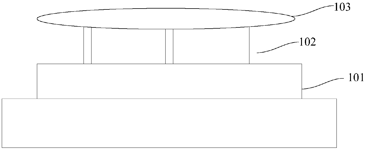
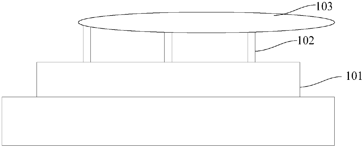
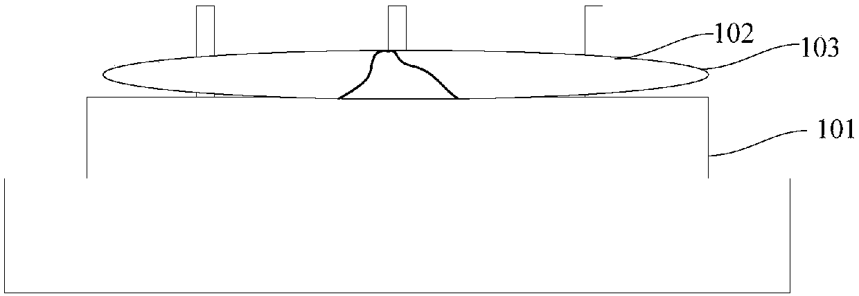
[0044] This embodiment provides an electrostatic discharge method for an electrostatic chuck. The electrostatic chuck 200 includes a chuck 201 and a wafer pin 202. The electrostatic chuck 200 is provided with a driving device. The wafer pin 202 can be driven by the driving device. The up and down reciprocating movement pushes up the wafer 203 from the carrying surface of the chuck 201 or places the wafer 203 on the carrying surface of the chuck 201. The lifting position of the wafer pin 202 in this embodiment includes a pre-desorption position H1 and a target position H2. The target position H2 is higher than the pre-desorption position H1, and the height of the pre-desorption position H1 is between The target position H2 is between 1 / 50 and 1 / 2 of the height, the pre-desorption position H1 is a position where the adsorption force between the wafer 203 and the electrostatic chuck 200 is basically overcome, and the target position H2 may be a position where the wafer is operated...

Embodiment 2

[0061] Such as Figure 8 As shown, this embodiment provides an electrostatic discharge device of the electrostatic chuck 200, and the electrostatic discharge device includes an electrostatic chuck 200, a power supply 204, and a processing unit 205.

[0062] The electrostatic chuck 200 is used to suck the wafer 203, and the electrostatic chuck 200 is provided with a wafer pin 202, and the wafer pin 202 is used to lift the wafer 203. The electrostatic chuck 200 includes a chuck 201 and a wafer pin 202. The electrostatic chuck 200 is provided with a driving device (not shown). The wafer pin 202 can reciprocate up and down under the drive of the driving device, so that the wafer The circle 203 is raised from the carrying surface of the chuck 201 or the wafer 203 is placed on the carrying surface of the chuck 201. The lifting position of the wafer pin 202 in this embodiment includes a pre-desorption position H1 and a target position H2. The target position H2 is higher than the pre-de...


PUM


Abstract

The invention provides an electrostatic discharge method and device for an electrostatic chuck, and the device comprises: an electrostatic chuck which is provided with a wafer pin for lifting a wafer,wherein the electrostatic chuck is provided with a power supply and used for providing a fixed reverse voltage for the wafer when receiving the first power supply signal and providing stepped reversevoltage which is progressively increased in steps for the wafer when receiving the second power supply signal; and a processing unit which is used for judging whether the wafer pin reaches the pre-desorption position or not in a preset time period after the wafer pin is started to lift the wafer, and sending a first power supply signal for providing fixed reverse voltage or a second power supplysignal for providing stepped reverse voltage which is increased progressively according to a judgment result. By setting the reverse voltage applied to the electrostatic chuck and the stepped reversevoltage increased in a stepped manner, the judgment time is increased, the problem of electrostatic residue of the wafer after etching in the process cavity is finished can be effectively solved, andthe risk that the wafer deviates and is broken by a wafer pin in the conveying process is reduced.

Description

Technical field [0001] The invention belongs to the field of semiconductor manufacturing equipment design, and particularly relates to an electrostatic discharge method and device for an electrostatic chuck. Background technique [0002] In the integrated circuit chip manufacturing industry, the entire process of processing wafers generally includes processes such as photolithography, etching, ion implantation, metal deposition, and core packaging. In the plasma etching process, the etching machine transfers the photoresist patterns such as lines, surfaces or holes produced by the photolithography process to the material under the photoresist faithfully to form the entire integrated circuit. Architecture. In the packaging field, the overall thinning of device wafers and back packaging also require plasma etching processes. The above process is usually completed by placing the wafer on a chuck in the reaction chamber of the semiconductor processing equipment to process the wafer...

Claims


Application Information

Patent Timeline
Patent Type & Authority Applications(China)
IPC IPC(8): H01L21/683
CPCH01L21/6833
Inventor 不公告发明人
Owner CHANGXIN MEMORY TECH INC
Why Eureka
Try Eureka