Wafer detection method, device and equipment

A detection method and wafer technology, which can be used in measurement devices, optical testing flaws/defects, semiconductor/solid-state device testing/measurement, etc., and can solve problems such as chromatic aberration, focus spot, and inflexible detection standards

Pending Publication Date: 2020-06-05
YANGTZE MEMORY TECH CO LTD
View PDF20 Cites 8 Cited by
  • Summary
  • Abstract
  • Description
  • Claims
  • Application Information

AI Technical Summary

Problems solved by technology

In the process of making wafers, it is inevitable that some wafers will have defects. For example, during the photolithography process, due to the uneven surface of the wafer, it will cause defects such as focusing spots and chromatic aberration.
[0004] However, when using the image detection method and detection standard that comes with WIS to perform defect detection on the pictures before and after photolithography of the wafer to determine the wafer with defects, due to the image detection method and inspection standards that come with WIS The inspection standard is very inflexible. In some scenarios, it is possible to determine some wafers with negligible small defects as unqualified wafers, or determine the defective wafers as qualified wafers, then according to the wafers obtained The chip has quality problems, which increases the production cost

Method used


Image

  • Wafer detection method, device and equipment
  • Wafer detection method, device and equipment
  • Wafer detection method, device and equipment

Examples


Embodiment Construction

[0072] In order to make the purpose, technical solutions and advantages of the embodiments of the present invention clearer, the technical solutions in the embodiments of the present invention will be clearly and completely described below in conjunction with the drawings in the embodiments of the present invention. Obviously, the described embodiments It is a part of embodiments of the present invention, but not all embodiments. Based on the embodiments of the present invention, all other embodiments obtained by persons of ordinary skill in the art without creative efforts fall within the protection scope of the present invention.

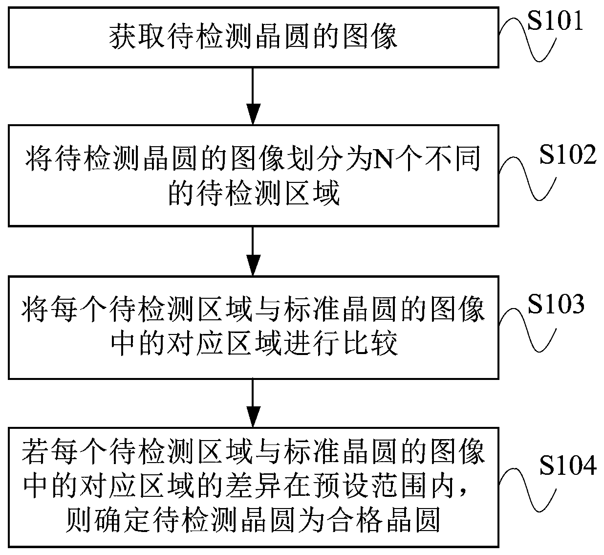
[0073] figure 1 The flow chart of the wafer detection method provided for an embodiment of the present invention, such as figure 1 As shown, the method of this embodiment may include:

[0074] S101. Acquiring an image of a wafer to be inspected.

[0075] In this embodiment, after the wafer passes through a process, defects may be caused in this...


PUM


Abstract

The embodiment of the invention provides a wafer detection method, device and equipment. The method comprises the following steps: acquiring an image of a to-be-detected wafer; comparing each to-be-detected area with a corresponding area in the standard wafer, wherein the standard wafer comprises N areas, each area of the standard wafer is in one-to-one correspondence with each to-be-detected area, and the position of the to-be-detected area in the to-be-detected wafer is the same as the position of the corresponding area in the standard wafer, and if the difference between each to-be-detectedarea and the corresponding area of the standard wafer is within a preset range, determining that the to-be-detected wafer is a qualified wafer. The judgment standards of different areas in the waferfor defects are different, and defect detection is performed on each to-be-detected area so that the defect detection of the wafer is more flexible, and the detection accuracy is higher. The problem in the prior art that when defects of the wafer are detected, the detection standard for detecting whether the defects exist in the wafer is inflexible and the detection result of whether the defects exist in the wafer is inaccurate is solved, and thus the production cost is reduced.

Description

technical field [0001] Embodiments of the present invention relate to the technical field of semiconductor manufacturing, and in particular to a wafer detection method, device and equipment. Background technique [0002] Wafer refers to the silicon chip used in the production of silicon semiconductor integrated circuits. It is the carrier used in the production of integrated circuits (IC). Therefore, the quality of the wafer directly affects the yield rate and manufacturing cost of the chip. In the process of making wafers, it is inevitable that some wafers will have defects. For example, during the photolithography process, due to the unevenness of the wafer surface, defects such as focusing spots and chromatic aberrations will be caused. Therefore, it is necessary to inspect the wafer to obtain a standard wafer. [0003] In the prior art, a wafer inspection system (wafer inspect system, WIS) is used to take pictures of the wafer before and after photolithography, and the ...

Claims


Application Information

Patent Timeline
Patent Type & Authority Applications(China)
IPC IPC(8): G01N21/95G06T7/00G06T7/90H01L21/66
CPCG01N21/9503G06T7/0004G06T7/90H01L22/12H01L22/20G06T2207/30148
Inventor 谢真良郑先意
Owner YANGTZE MEMORY TECH CO LTD
Why Eureka
Try Eureka