

Super junction device and manufacturing method thereof
A manufacturing method and super-junction technology, applied in semiconductor/solid-state device manufacturing, semiconductor devices, electrical components, etc., can solve the problems of net doping concentration reduction, device performance degradation, etc., and achieve compensation for doping loss, elimination of leakage, and high Effect of doping concentration
- Summary
- Abstract
- Description
- Claims
- Application Information
AI Technical Summary
Problems solved by technology
Method used
Image

Examples
no. 1 example
[0058] The super junction device of the first embodiment of the present invention:
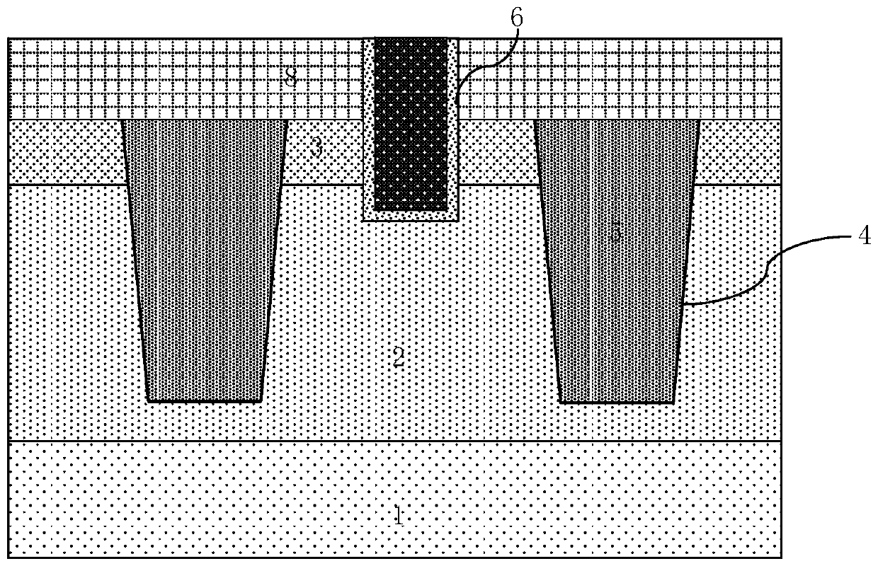
[0059] Such as figure 1 As shown, it is a schematic structural diagram of the super junction device of the first embodiment of the present invention; the device unit area of the super junction device of the first embodiment of the present invention includes:
[0060] A super junction composed of alternately arranged P-type pillars 5 and N-type pillars, a super junction unit is composed of one P-type pillar 5 and one adjacent N-type pillar.
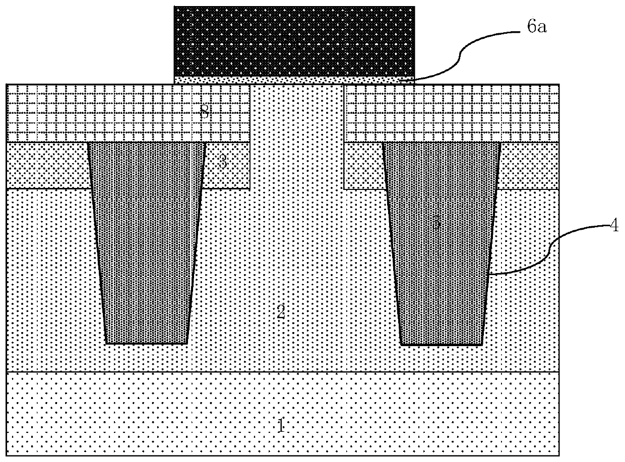
[0061] The P-type column 5 is composed of a P-type epitaxial layer filled in the super junction trench 4, and the N-type column is composed of a first N-type epitaxial layer 2 located between the P-type columns 5. The super junction A junction trench 4 is formed in the first N-type epitaxial layer 2 ; surface defects generated by filling the super junction trench 4 are easily formed on the surface of the super junction. The formation of surface defects...
PUM
 Abstract
Description
Claims
Application Information