Packaging method of GaAs-based LED lamp bead

A technology of LED lamp beads and packaging methods, which is applied in the field of optoelectronics, can solve the problems of conductive silver glue leakage and other problems, and achieve the effect of eliminating leakage, avoiding leakage, and simple operation

Active Publication Date: 2020-11-24
SHANDONG INSPUR HUAGUANG OPTOELECTRONICS
View PDF5 Cites 0 Cited by
  • Summary
  • Abstract
  • Description
  • Claims
  • Application Information

AI Technical Summary

Problems solved by technology

[0006] In view of the shortage of current leakage caused by conductive silver glue in the existing GaAs-based LED lamp bead packaging method, the present invention provides a GaAs-based LED that is easy

Method used


Image

  • Packaging method of GaAs-based LED lamp bead
  • Packaging method of GaAs-based LED lamp bead

Examples


Example Embodiment

[0027] Example 1:

[0028] A packaging method for GaAs-based LED lamp beads, comprising the following steps:
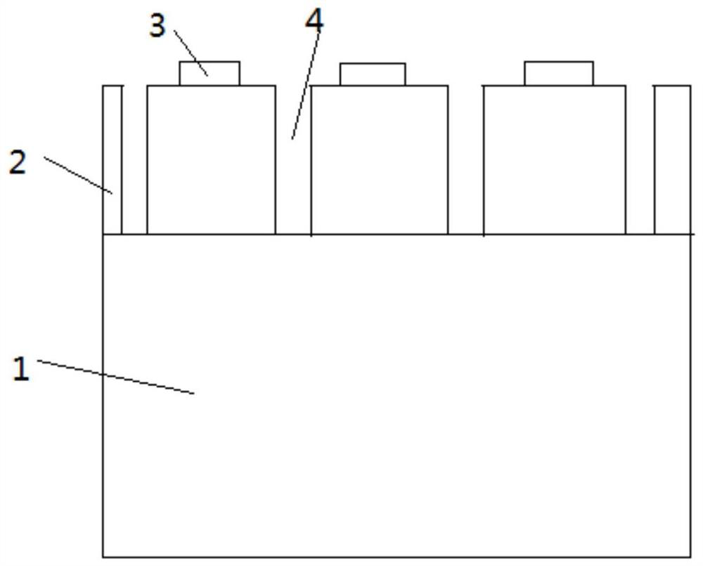
[0029] (1) A GaAs-based light-emitting diode chip epitaxial layer is grown on a GaAs substrate 1, and the P-electrode 3 and N-electrode of the light-emitting diode chip are prepared by conventional P-side metal deposition, photolithography P-electrode, thinning, and N-side metal deposition methods 5;

[0030] (2) P-cutting the GaAs-based light-emitting diode chip obtained in step (1), such as figure 1 As shown, a diamond knife is used to form a strip-shaped dicing track 4 around the P electrode 3, and the cycle of the dicing track 4 is consistent with the cycle of the P electrode 3 and the dicing track 4 does not completely divide the GaAs-based light-emitting diode chip (the epitaxial layer has been cut through And cut to the substrate), carry out the conventional test to the cut chip to obtain the chip photoelectric parameters, and can adopt the conventional metho...

Example Embodiment

[0034] Example 2:

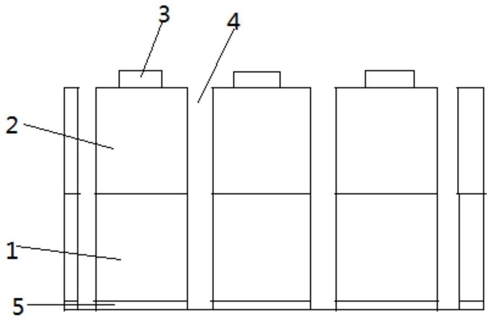
[0035] A packaging method for GaAs-based LED lamp beads, as shown in Embodiment 1, the difference is that in step (2), the cutting depth is 1 / 4 of the chip thickness, and the chip thickness here includes the thickness of the GaAs substrate and the epitaxial layer. thickness;

[0036] The width of the dicing lanes 4 is 25 μm.

Example Embodiment

[0037] Example 3:

[0038] A packaging method for GaAs-based LED lamp beads, as shown in Embodiment 1, the difference is that the thickness of the magnetic packaging metal substrate is 30 μm.


PUM

PropertyMeasurementUnit
Widthaaaaaaaaaa
Thicknessaaaaaaaaaa
Thicknessaaaaaaaaaa

Abstract

The invention relates to a packaging method of a GaAs-based LED lamp bead, which belongs to the field of photoelectrons, and comprises the following steps: growing a GaAs-based light emitting diode chip epitaxial layer on a GaAs substrate, and preparing a P electrode and an N electrode through adoption of a conventional method; carrying out P-surface cutting on the chip, forming a strip-shaped cutting channel around the P electrode, and not completely dividing the chip by the cutting channel; bonding the N surface with a magnetic packaging metal substrate through a conductive silver adhesive;completely cutting the chip along the cutting channel, and connecting the packaging metal substrate with the packaging support in a magnetic attraction mode; connecting the P electrode with the positive electrode of the packaging support through a metal wire, and then coating the periphery of the packaging metal substrate with epoxy resin glue for filling and packaging; and putting the packaging support into a drying oven to heat and solidify the glue to obtain the packaged GaAs-based light emitting diode chip lamp bead. The method is easy to operate, and the situation that the conductive silver adhesive covers the epitaxial layer on the side face of the GaAs-based light emitting diode chip to cause lamp bead electric leakage is eradicated.

Description

technical field [0001] The invention relates to a method for packaging GaAs-based LED lamp beads, which belongs to the field of optoelectronic technology. Background technique [0002] LED is a new light source for lighting in the 21st century. Under the same brightness, the power consumption of semiconductor lamps is only 1 / 10 of that of ordinary incandescent lamps, but the life span can be extended by 100 times. The LED device is a cold light source with high luminous efficiency, low working voltage, low power consumption, small size, flat packaging, easy to develop thin and light products, strong structure and long life. The light source itself does not contain harmful substances such as mercury and lead. No infrared and ultraviolet pollution, no pollution to the outside world during production and use. Therefore, semiconductor lamps have the characteristics of energy saving, environmental protection, and long life. Just like transistors replace electronic tubes, semicon...

Claims


Application Information

Patent Timeline
IPC IPC(8): H01L33/48H01L33/62H01L33/54
CPCH01L33/483H01L33/54H01L33/62H01L2933/0033H01L2933/005H01L2933/0066
Inventor 李晓明任忠祥王成新
Owner SHANDONG INSPUR HUAGUANG OPTOELECTRONICS
Why Eureka
Try Eureka