Integrated circuit ESD protection circuit

An ESD protection, integrated circuit technology, applied in the field of ESD protection design, can solve the problems of low turn-on voltage, easy breakdown and failure of gate oxide layer, large area, etc.

Pending Publication Date: 2020-06-09
伟芯科技(绍兴)有限公司
View PDF0 Cites 0 Cited by
  • Summary
  • Abstract
  • Description
  • Claims
  • Application Information

AI Technical Summary

Problems solved by technology

[0011] In order to solve the above problems of high turn-on voltage of integrated circuit ESD devices, easy breakdown and failure of the gate oxide layer, and large area, the technical method of the present invention is proposed to provide a lower turn-on voltage while avoiding the breakdown of the oxide layer Ineffective and area-saving technical method

Method used


Image

  • Integrated circuit ESD protection circuit
  • Integrated circuit ESD protection circuit
  • Integrated circuit ESD protection circuit

Examples


Embodiment Construction

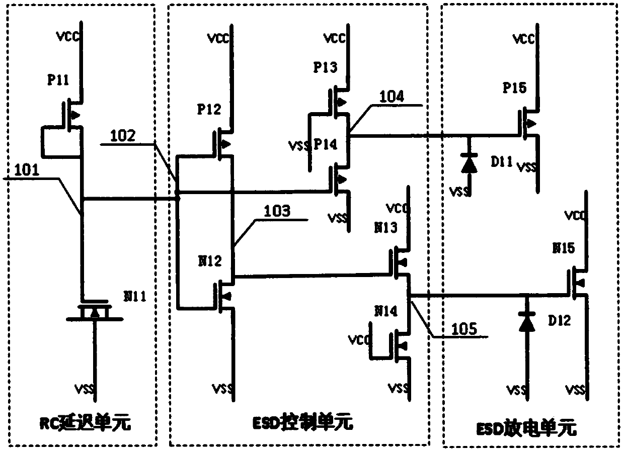
[0027] Specific embodiments of the present invention are as attached figure 1 shown.

[0028] It mainly includes three parts, which are RC delay unit, ESD control unit and ESD discharge unit.

[0029] The RC delay unit is composed of an equivalent capacitance N11 composed of NMOS and an equivalent resistance P11 composed of PMOS, wherein the source and substrate of the equivalent resistance P11 are connected to the power supply VCC, and the gate and drain are connected to the output point 101 , so the P11 device is in the normally open state of the channel, forming a PMOS channel resistance. The resistance formed by this method has a smaller area than the resistance formed by polysilicon, which can save layout area and reduce chip cost. The source, drain and substrate of the equivalent capacitor N11 are all connected to the ground VSS, and the gate is connected to the output point 101, so the equivalent capacitor is formed by the gate oxide layer of the NMOS N11. The RC st...


PUM


Abstract

The invention relates to the technical field of integrated circuit (IC) electro-static discharge (ESD) protection design in microelectronics, and provides an ESD protection circuit with high reliability, low turn-on voltage and low cost. A PMOS (positive channel metal oxide semiconductor) and NMOS (negative channel metal oxide semiconductor) simultaneous discharge mode is adopted. The gate drivingsignal of an ESD discharge tube is generated by conduction and voltage division of the PMOS device and the NMOS device. The time delay of the driving signal is controlled by R (resistor) C (capacitor), R is realized by a PMOS device or an NMOS device. A reverse conducting diode (D) is connected in parallel to the gate of the discharge device PMOS and NMOS, and the gate reliability is enhanced. According to the design, the reliability of the ESD protection circuit is improved, the turn-on voltage is reduced, and the chip cost is reduced.

Description

technical field [0001] The invention relates to an integrated circuit ESD protection circuit, which is suitable for the electrostatic discharge protection design of the integrated circuit, and is especially suitable for the ESD protection design which requires a lower turn-on voltage while realizing high reliability while saving area and reducing cost. Background technique [0002] As the level of integrated circuit manufacturing technology has entered the deep submicron era and nanometer era, the MOS transistors in the integrated circuit all adopt the lightly doped structure LDD (Lightly Doped Drain); the silicide is covered on the diffusion area of ​​the MOS transistor; the polycrystalline compound process It is used to reduce the series resistance of the gate polysilicon; and the thickness of the gate oxide layer of the MOS transistor is getting thinner and the channel length is getting smaller and smaller. These improvements have improved the integration of the chip, inc...

Claims


Application Information

Patent Timeline
Patent Type & Authority Applications(China)
IPC IPC(8): H02H9/04
CPCH02H9/046
Inventor 马树永
Owner 伟芯科技(绍兴)有限公司
Why Eureka
Try Eureka