
An organic light emitting diode display and method of manufacturing same

A technology for light-emitting diodes and displays, which is applied in the manufacture of semiconductor/solid-state devices, electric solid-state devices, semiconductor devices, etc., can solve the problems of metal layer residues and large capacitor capacitance, and achieve the effect of avoiding metal residues

Active Publication Date: 2020-06-12
WUHAN CHINA STAR OPTOELECTRONICS SEMICON DISPLAY TECH CO LTD
View PDF5 Cites 2 Cited by
  • Summary
  • Abstract
  • Description
  • Claims
  • Application Information

AI Technical Summary

Problems solved by technology

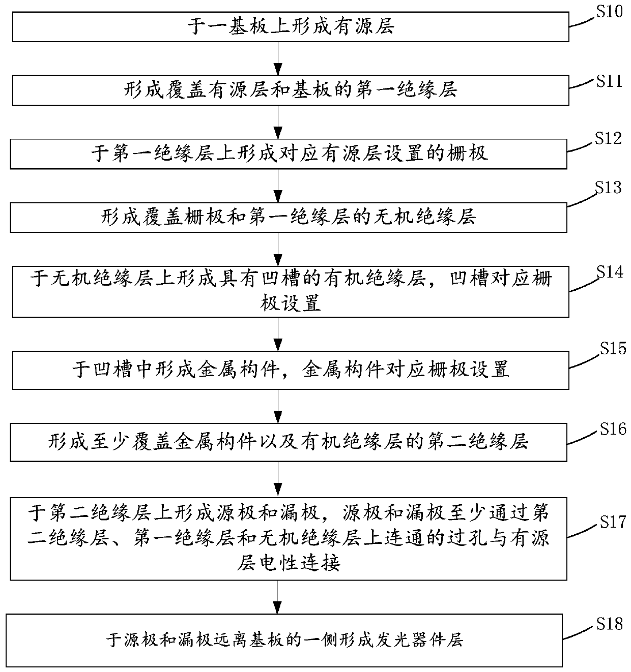
[0004] The purpose of this application is to provide an organic light emitting diode display and its manufacturing method, to solve the problem of residual etching of the metal layer used to form the metal member at the steep slope, while ensuring the capacitance of the capacitor composed of the gate and the metal member larger

Method used


Image

  • An organic light emitting diode display and method of manufacturing same
  • An organic light emitting diode display and method of manufacturing same
  • An organic light emitting diode display and method of manufacturing same

Examples


Embodiment Construction

[0044] The technical solutions in the embodiments of the present application will be clearly and completely described below in conjunction with the drawings in the embodiments of the present application. Apparently, the described embodiments are only some of the embodiments of this application, not all of them. Based on the embodiments in this application, all other embodiments obtained by those skilled in the art without making creative efforts belong to the scope of protection of this application.

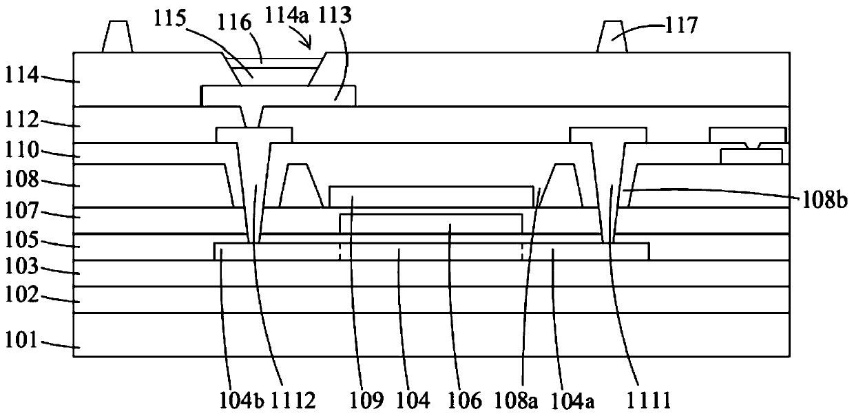
[0045] see figure 1 , which is a schematic structural diagram of an organic light emitting diode display according to an embodiment of the present application. The organic light emitting diode display 10 is a top emission type organic light emitting diode display, and it can be understood that the organic light emitting diode display 10 may also be a bottom emission type organic light emitting diode display. The OLED display 10 includes a substrate 101, a barrier layer 102, a b...


PUM

PropertyMeasurementUnit
Thicknessaaaaaaaaaa
Thicknessaaaaaaaaaa

Abstract

The invention provides an organic light emitting diode display and a manufacturing method thereof. An inorganic insulating layer covering a grid electrode is formed; an organic insulating layer is formed on the inorganic insulating layer to achieve a planarization effect; the problem of metal residue during etching of a subsequently formed metal layer due to an abrupt slope is avoided; a groove isformed in the position, corresponding to the grid electrode, of the organic insulating layer, a metal component used for forming a capacitor with the grid electrode is formed in the groove and arranged corresponding to the grid electrode, the distance between the grid electrode and the metal component is reduced, and the capacitance of the capacitor composed of the grid electrode and the metal component is large.

Description

technical field [0001] The present application relates to the field of display technology, in particular to an organic light emitting diode display and a manufacturing method thereof. Background technique [0002] Organic Light-Emitting Diode (OLED), due to its advantages of light weight, self-illumination, wide viewing angle, low driving voltage, high luminous efficiency, low power consumption and fast response, has been widely used. [0003] In the traditional technology, the scanning lines in OLED displays are made of molybdenum. Due to the high resistivity of molybdenum, in wide-screen OLED displays, the scanning lines made of molybdenum will cause delays in gate drive signals. Obviously, it is necessary to use a metal material with a small resistance to solve the problem of delay of the gate driving signal, and the metal material with a small resistivity includes aluminum. When the metal layer with lower resistivity is patterned by dry etching to form the gate of the t...

Claims


Application Information

Patent Timeline
IPC IPC(8): H01L51/56H01L51/52H01L27/32
CPCH10K59/122H10K50/80H10K50/84H10K71/00H10K59/1213H10K59/123H10K59/124H10K59/1201
Inventor 杨薇薇陈诚
Owner WUHAN CHINA STAR OPTOELECTRONICS SEMICON DISPLAY TECH CO LTD
Learn More