A kind of semiconductor device and its manufacturing method

A manufacturing method and semiconductor technology, applied in the direction of semiconductor/solid-state device manufacturing, semiconductor devices, electrical components, etc., can solve problems such as affecting the performance of semiconductor devices and easily generating leakage current, and achieve the effect of improving performance and avoiding leakage current.

Active Publication Date: 2017-02-08
SEMICON MFG INT (SHANGHAI) CORP
View PDF4 Cites 0 Cited by
  • Summary
  • Abstract
  • Description
  • Claims
  • Application Information

AI Technical Summary

Problems solved by technology

[0009] In the prior art, the aforementioned metal residues 1051 tend to cause the final semiconductor device to easily generate leakage current during operation, seriously affecting the performance of the semiconductor device

Method used


Image

  • A kind of semiconductor device and its manufacturing method
  • A kind of semiconductor device and its manufacturing method
  • A kind of semiconductor device and its manufacturing method

Examples


Embodiment 1

[0047] Below, refer to Figure 2A-Figure 2F and image 3 , to describe the detailed steps of an exemplary method of the semiconductor device manufacturing method proposed by the present invention. in, Figure 2A-Figure 2F A schematic cross-sectional view of the graphics formed in each step of the manufacturing method of the semiconductor device proposed by the present invention; image 3 It is a flowchart of a manufacturing method of a semiconductor device proposed by the present invention.

[0048] The method for manufacturing a semiconductor device according to an embodiment of the present invention includes the following steps:

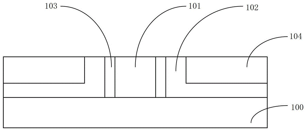
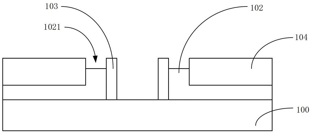
[0049] Step 1: Provide a semiconductor substrate 200, on which a dummy gate 201, a contact etch stop layer (CESL) 202, a gate sidewall 203 and an interlayer dielectric layer 204 are formed, such as Figure 2A shown. Of course, the semiconductor substrate 200 may also include STI, source / drain and other structures (not shown in the figure), whi...

Embodiment 2

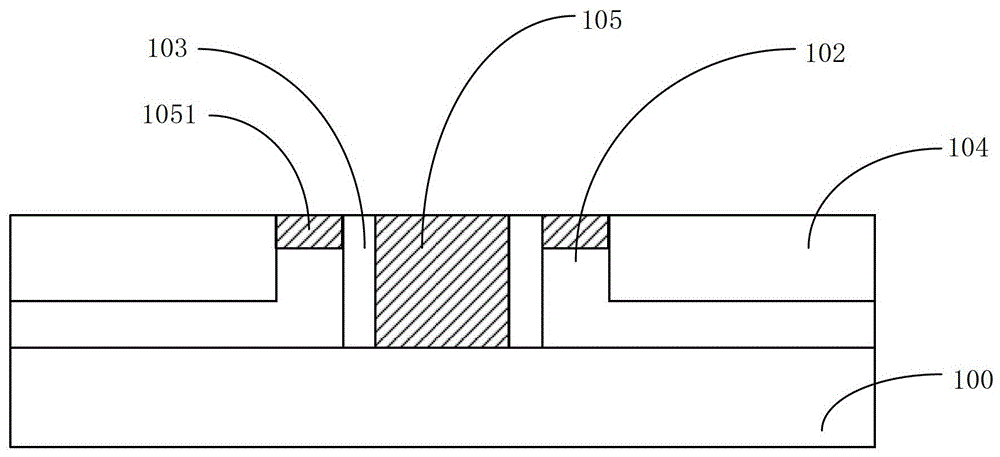
[0080] An embodiment of the present invention provides a semiconductor device, such as Figure 2F As shown, the semiconductor device includes a semiconductor substrate 200, a metal gate 206 located on the semiconductor substrate 200, a contact hole etch barrier layer 202, a gate sidewall 203 and an interlayer dielectric layer 204, wherein the The semiconductor device further includes: a protection layer 2051 located above the contact hole etch barrier layer 202 , and the protection layer 2051 is on the same plane as the interlayer dielectric layer 204 .

[0081] Wherein, the protection layer 2051 and the interlayer dielectric layer 204 are on the same plane, which refers to the case where the semiconductor substrate 200 is placed horizontally.

[0082] Further, the thickness of the protective layer 2051 is 3nm-30nm.

[0083] Further, the material of the protection layer 2051 is silicon oxide.

[0084] The semiconductor device provided by the embodiment of the present inventi...


PUM


Abstract

The invention provides a semiconductor device and a manufacturing method thereof, and relates to the technical field of semiconductors. According to the manufacturing method of the semiconductor device of the invention, the process of forming a protective layer above a contact hole etch stop layer is added before the process step of removing a dummy gate. According to the method, formation of a recess above the contact hole etch stop layer in the process of removing the dummy gate is avoided, formation of metal residue above the contact hole etch stop layer in the process of forming a metal gate is avoided, generation of leakage current is avoided to a certain extent, and the performance of the semiconductor device is improved. According to the semiconductor device of the invention, a protective layer is formed above a contact hole etch stop layer. As the semiconductor device has the protective layer, that metal residue is not formed above the contact hole etch stop layer is ensured, generation of leakage current is avoided to a certain extent, and the performance of the semiconductor device is improved.

Description

technical field [0001] The invention relates to the technical field of semiconductors, in particular to a semiconductor device and a manufacturing method thereof. Background technique [0002] High-K metal gate (HKMG) technology is an important technology in the semiconductor field. Compared with ordinary gate technology, HKMG technology can greatly improve the performance of semiconductor devices. In the prior art, in the process of removing dummy gates in the manufacturing method of semiconductor devices using high-k metal gate technology, part of the contact hole etch stop layer (CESL) is often removed improperly. A recess is formed above, which leads to the formation of metal residues at the recessed position during the subsequent process of forming the metal gate. The metal residues in the corresponding positions often lead to the occurrence of leakage current, which seriously affects the performance of semiconductor devices. [0003] Below, combine Figure 1A to Figu...

Claims


Application Information

Patent Timeline
Patent Type & Authority Patents(China)
IPC IPC(8): H01L21/28H01L29/423
CPCH01L21/28008H01L29/423
Inventor 韩秋华
Owner SEMICON MFG INT (SHANGHAI) CORP
Why Eureka
Try Eureka