Dispensing method, bonding plate and crystal support for silicon wafer manufacturing

A bonding board and glue dispensing technology, which is applied to working accessories, manufacturing tools, fine working devices, etc., can solve the problems of high rate of defective products on the edge of silicon wafers, overflowing glue, bad glue layer, air bubbles, etc., to ensure the adhesion Add strength, eliminate bad product rate, avoid the effect of glue overflow

Pending Publication Date: 2020-06-19
CHUXIONG LONGI SILICON MATERIALS CO LTD
View PDF0 Cites 0 Cited by
  • Summary
  • Abstract
  • Description
  • Claims
  • Application Information

AI Technical Summary

Problems solved by technology

Due to differences in personnel skills during the application process, empty glue, poor glue overflow and bubbles inside the glue layer will occur after the silicon rods are bonded
When the steel wire is cut to the empty glue, overflow glue or bubbles in the glue layer of the silicon rod, the steel wire will be unevenly stressed and shake, causing a high rate of defective products on the edge of the silicon wafer

Method used


Image

  • Dispensing method, bonding plate and crystal support for silicon wafer manufacturing
  • Dispensing method, bonding plate and crystal support for silicon wafer manufacturing
  • Dispensing method, bonding plate and crystal support for silicon wafer manufacturing

Examples


Embodiment 1

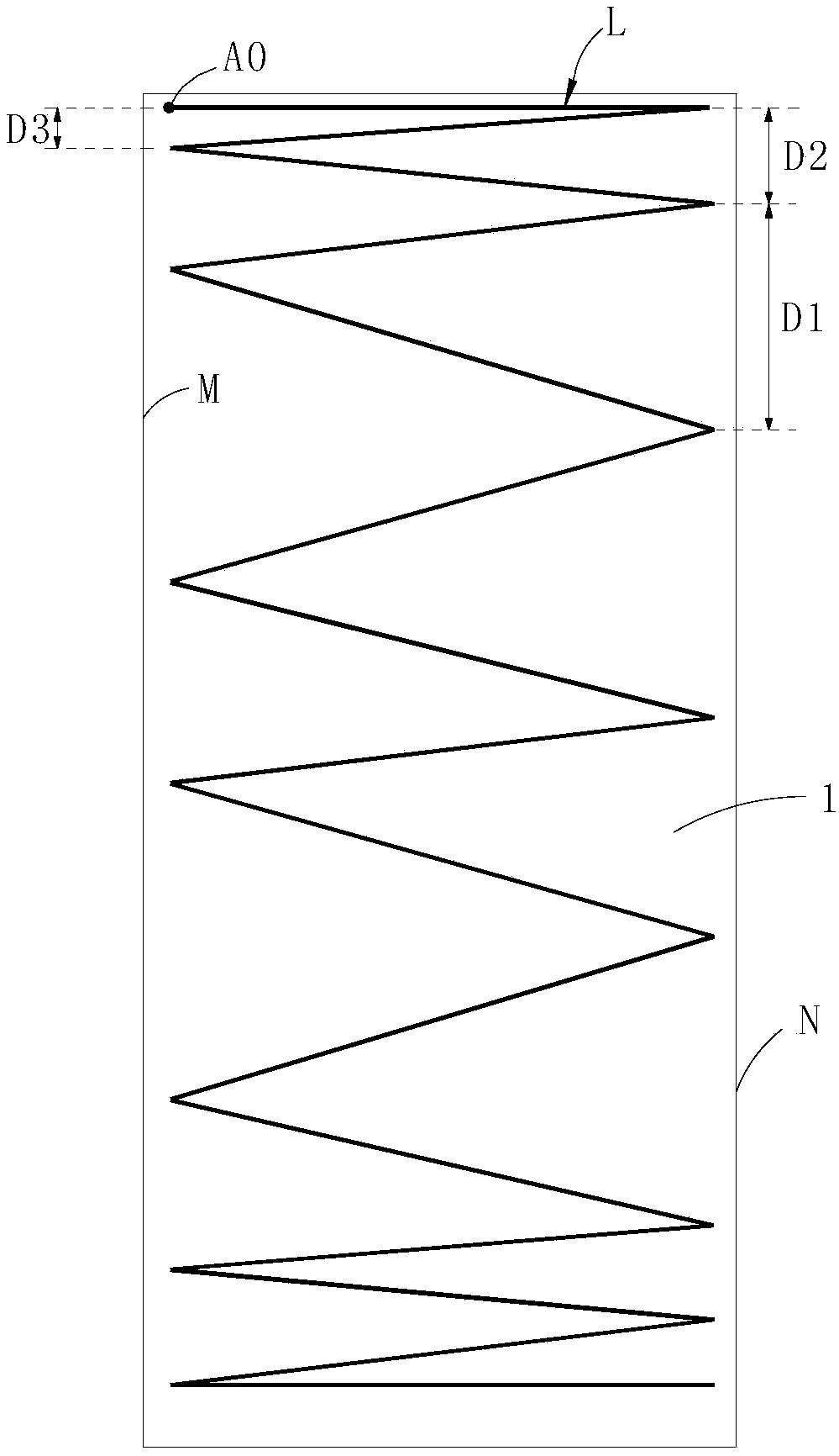
[0030] refer to figure 1 , the dispensing method of the present embodiment mainly comprises the following steps:

[0031] S01. Provide a substrate 1 to be dispensed, and the substrate 1 includes a first side line M and a second side line N oppositely arranged.

[0032] Wherein, the dispensing starting point A0 is close to the first side line M, for example, the first side line M and the second side line N are respectively located on both sides of the width direction of the substrate 1 and extend along the length direction of the substrate 1 . The substrate here can be a crystal holder or an adhesive board.

[0033] S02 , sequentially coating a plurality of dispensing segments L on the substrate 1 to form a dispensing pattern L0 until the starting point and the ending point of the dispensing pattern L0 are separated by a predetermined distance in the length direction of the first side line M.

[0034] In the dispensing pattern L0, the starting point of each dispensing segmen...

Embodiment 2

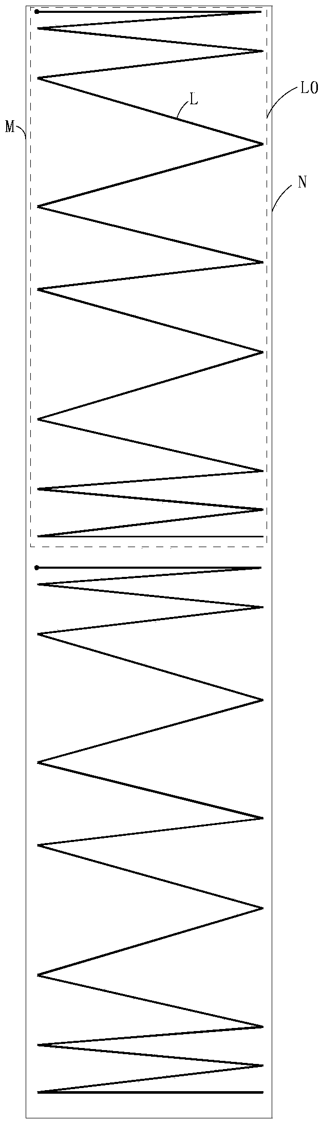
[0042] Such as figure 2 As shown, different from Embodiment 1, there are two dispensing patterns L0 on the substrate of this embodiment,

[0043] The length of each dispensing pattern L0 (the dimension along the length direction of the first side line M) matches the length of two short silicon rods, the length of a single short silicon rod is about 345mm, and the two short silicon rods pass through respectively A dispensing pattern L0 is spliced ​​on the substrate 1 to form a combined silicon rod with a length of about 690mm. Therefore, the length of each dispensing pattern L0 should not be greater than but close to 345mm, that is, the predetermined distance should not be greater than but close to 345mm.

[0044] On the basis of embodiment 1, the dispensing method for silicon wafer production of the present embodiment needs to repeatedly make the next dispensing pattern L0, and also includes the following steps:

[0045] S03. Select a new point near the start point or end po...

Embodiment 3

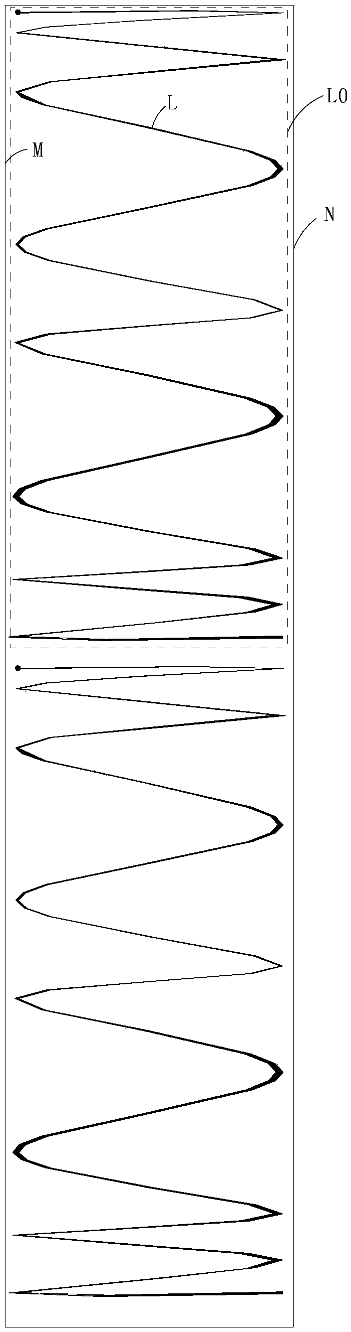
[0051] Such as image 3 As shown, different from the above embodiments, at least one dispensing segment L of this embodiment can be arranged in an arc, and even preferably each dispensing segment L can be an arc. Finally, each dispensing pattern L0 is Squiggly. The connection transition between the dispensing sections L is also an arc transition, which can increase the distance between the two dispensing sections and better prevent glue overflow.

[0052] In summary, the present invention forms a dispensing pattern formed by end-to-end connection of several dispensing sections by dispensing glue on various substrates, such as bonding boards or crystal holders, according to a predetermined track, and the glue line layer after lamination can maintain Very good uniformity, not only can avoid glue overflow, but also can easily discharge the air between the dispensing sections, there will be no empty glue or glue layer bubbles, and it can eliminate the edge of the silicon wafer ca...


PUM

PropertyMeasurementUnit
lengthaaaaaaaaaa

Abstract

The invention discloses a dispensing method for manufacturing a silicon wafer. The method comprises the following steps of providing a substrate to be dispensed, wherein the substrate comprises a first side line and a second side line which are oppositely arranged; sequentially coating a plurality of dispensing sections on the substrate to form a dispensing pattern until the starting point and theterminal point of the dispensing pattern are spaced by a preset distance in the length direction of the first side line; in the dispensing pattern, the starting point of each dispensing section is close to the first side line or the second side line, the terminal point of each dispensing section is close to the second side line or the first side line, and the terminal point of the previous dispensing section is the starting point of the next dispensing section. The laminated glue line layer can keep good uniformity, glue overflow can be avoided, air between dispensing sections can be conveniently exhausted, empty glue or glue layer bubbles cannot occur, the defective rate of the edge surface of the silicon wafer caused by uneven stress of a steel wire can be eliminated, and the number ofthe dispensing patterns on the substrate and the glue line spacing of the dispensing patterns can be customized according to the rod length of the silicon rod.

Description

technical field [0001] The invention relates to the technical field of single crystal slice manufacture, in particular to a glue dispensing method, a bonding plate and a crystal support for making silicon wafers. Background technique [0002] With the continuous development of the world economy, the demand for high-efficiency energy in modernization is increasing. Photovoltaic power generation, as one of the main energy sources for green energy and sustainable development of human beings, has been increasingly valued and vigorously developed by countries all over the world. As a basic material for photovoltaic power generation, monocrystalline silicon wafers have extensive market demand. [0003] Before silicon wafers are formed by wire cutting using diamond wires, silicon rods need to be bonded first. The bonding process includes bonding the bonding board to the crystal holder, and bonding the silicon rod to the bonding board, and finally the wire cutting process is perfor...

Claims


Application Information

Patent Timeline
Patent Type & Authority Applications(China)
IPC IPC(8): B28D7/00B28D7/04B28D5/04
CPCB28D5/0058B28D5/0082B28D5/045
Inventor 朱延松陆建虎张开增周化吉
Owner CHUXIONG LONGI SILICON MATERIALS CO LTD
Why Eureka
Try Eureka