
Semiconductor workshop clean room

A semiconductor and clean room technology, applied in the field of clean rooms, can solve the problems affecting the cleanliness of the external large-scale clean space and the disturbance of airflow in the external large-scale clean space, achieve good filtering effect and the safety of filtering and processing operations, and improve the overall cleanliness. the effect of improving air cleanliness

Active Publication Date: 2020-06-19
上海振南工程咨询监理有限责任公司
View PDF6 Cites 0 Cited by
  • Summary
  • Abstract
  • Description
  • Claims
  • Application Information

AI Technical Summary

Problems solved by technology

[0004] In the above-mentioned prior art, because the distance between the bottom of the partition and the raised floor is at least 2m, and the air pressure in the clean micro-environment structure is greater than that in the large clean space outside it, the clean micro-environment structure will flow outward to the large-scale clean space. Blowing airflow in the clean space, and the blowing airflow is turbulent flow or eddy current, which causes the flow direction of the airflow in the large external clean space to be disordered, which seriously affects the cleanliness of the large external clean space. There is room for improvement in the existing technology

Method used


Image

  • Semiconductor workshop clean room
  • Semiconductor workshop clean room
  • Semiconductor workshop clean room

Examples


Embodiment Construction

[0036] The present invention will be described in further detail below in conjunction with the accompanying drawings.

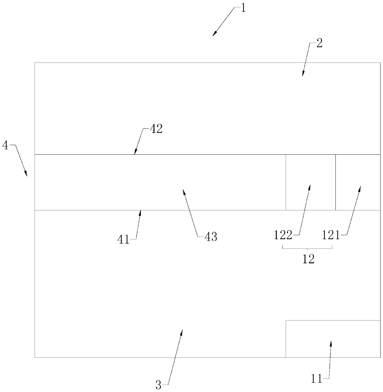
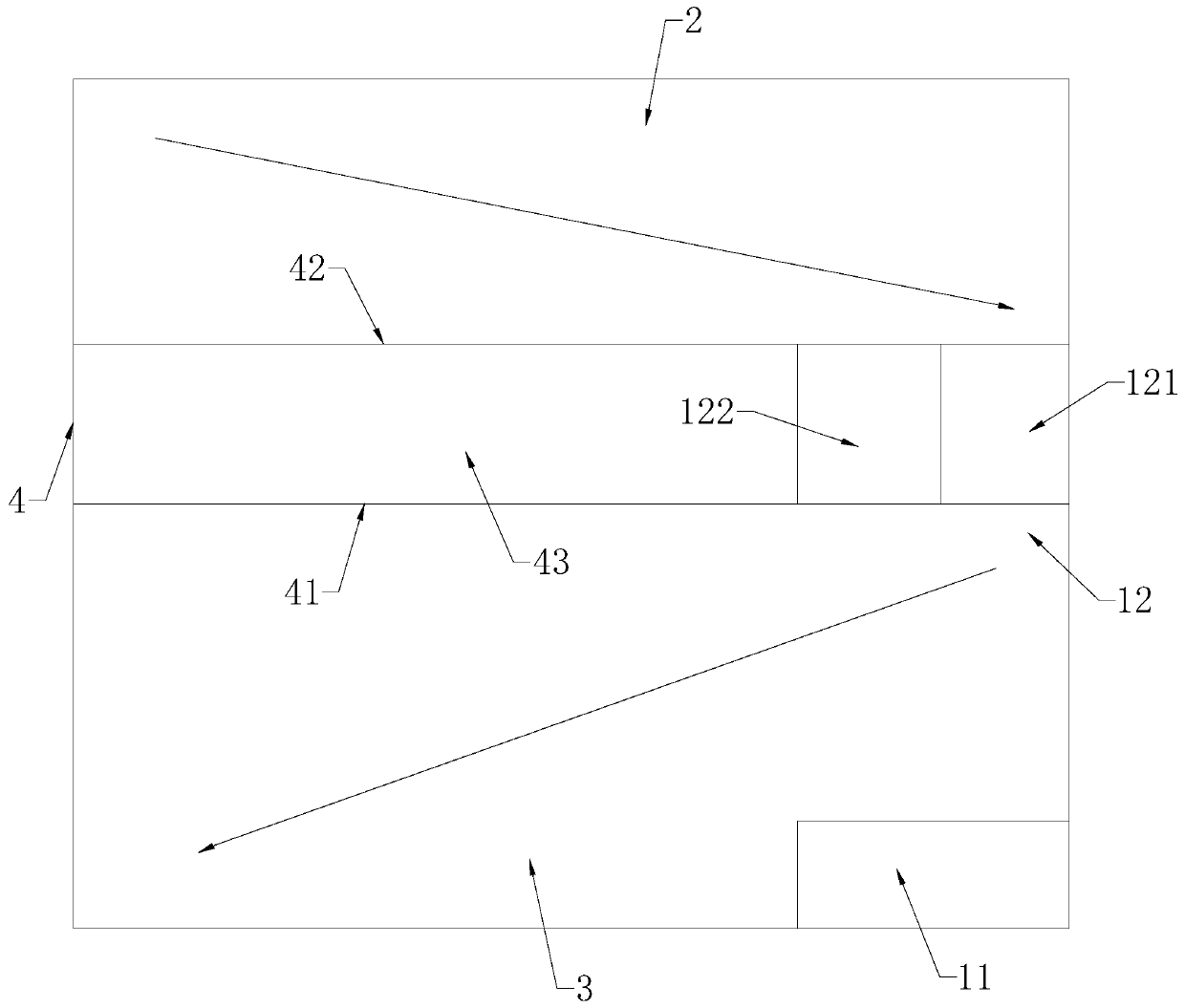
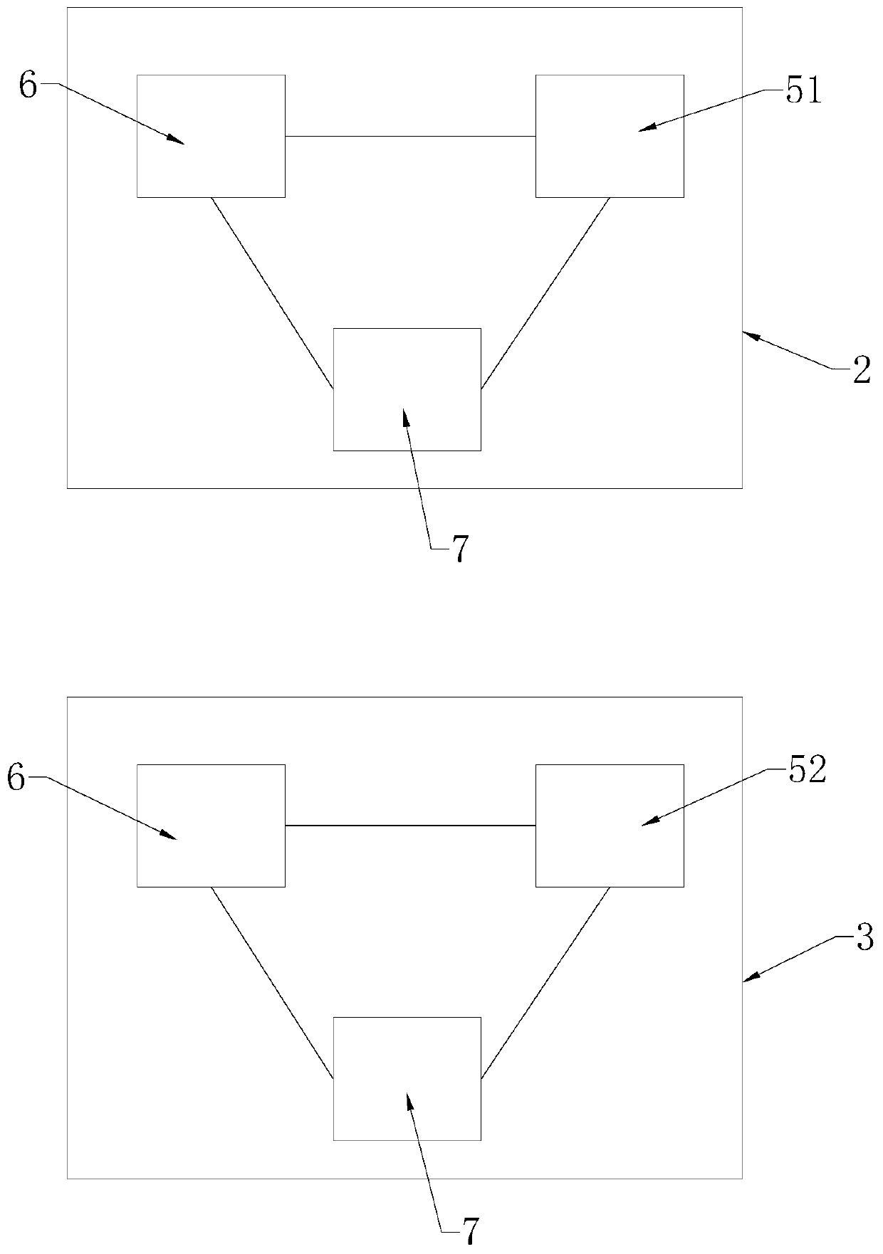
[0037] Such as figure 1 As shown, a clean room of a semiconductor plant includes a clean studio 1, and the clean studio 1 includes a clean operation area 2 and a processing service area 3, and the clean operation area 2 and the processing service area 3 are respectively used to realize high-precision processing operations And the pre-semiconductor process processing operation, and the clean operation area 2 and the processing service area 3 are separated by a separation area 4. The separation area 4 achieves the purpose of blocking the clean operation area 2 and the processing service area 3 through the airflow wall. combine figure 1 and image 3 As shown, while separating the clean operation area 2 and the processing service area 3, the clean operation area 2 and the processing service area 3 are also provided with an air supply system 6, a return air syst...


PUM


Abstract

The invention discloses a semiconductor workshop clean room, and relates to the technical field of clean rooms. The semiconductor workshop clean room comprises a clean working room, an air supply system, an air return system and a filtering system are arranged in the clean working room, the clean working room comprises a clean operation area and a processing service area, and a compartmentation area is arranged between the clean operation area and the processing service area; the compartmentation area comprises a vertical air supply area and a horizontal air supply area, a longitudinal air flow wall and a transverse air flow wall are formed in the vertical air supply area and the horizontal air supply area respectively, and an interval is formed between the longitudinal air flow wall and the transverse air flow wall, a vector air supply system and a one-way air supply system are arranged in the clean operation area, and a turbulent flow air supply system is arranged in the processing service area. The clean operation area and the processing service area achieve the purpose of limiting turbulent flow or vortex through the compartmentation area between the clean operation area and the processing service area and the air supply system, the air return system and the filtering system which are independent of each other, and therefore the purpose of improving the air cleanliness in the clean room is achieved.

Description

technical field [0001] The invention relates to the technical field of clean rooms, in particular to a clean room of a semiconductor workshop. Background technique [0002] Semiconductors refer to materials whose electrical conductivity is between conductors and insulators at room temperature, and are widely used in consumer electronics, communication systems, and medical instruments. Dust-free clean room, also known as clean room, clean room or dust-free workshop, can effectively control the indoor or factory air cleanliness, temperature and humidity, and air flow direction and other factors that affect the production process, and can meet the precision machinery industry, The semiconductor industry has strict requirements on the working environment. [0003] The existing authorized notification number is the Chinese patent CN103206101B, which discloses a clean room for semiconductor workshops, including a large clean space, which is equipped with a fresh air delivery syst...

Claims


Application Information

Patent Timeline
IPC IPC(8): E04H5/02F24F7/007F24F13/28B08B5/02
CPCB08B5/02E04H5/02F24F7/007F24F13/28
Inventor 王峻毅洪震
Owner 上海振南工程咨询监理有限责任公司
Learn More