Preparation method of interdigital electrode
A technology of interdigitated electrodes and carbon layers, which is applied to electrical components, impedance networks, etc., can solve the problems of large metal wires, poor adhesion, and collapsed patterns, so as to improve adhesion, improve molding accuracy and quality, and improve The effect of uniformity
- Summary
- Abstract
- Description
- Claims
- Application Information
AI Technical Summary
Problems solved by technology
Method used
Image
Examples
no. 1 example
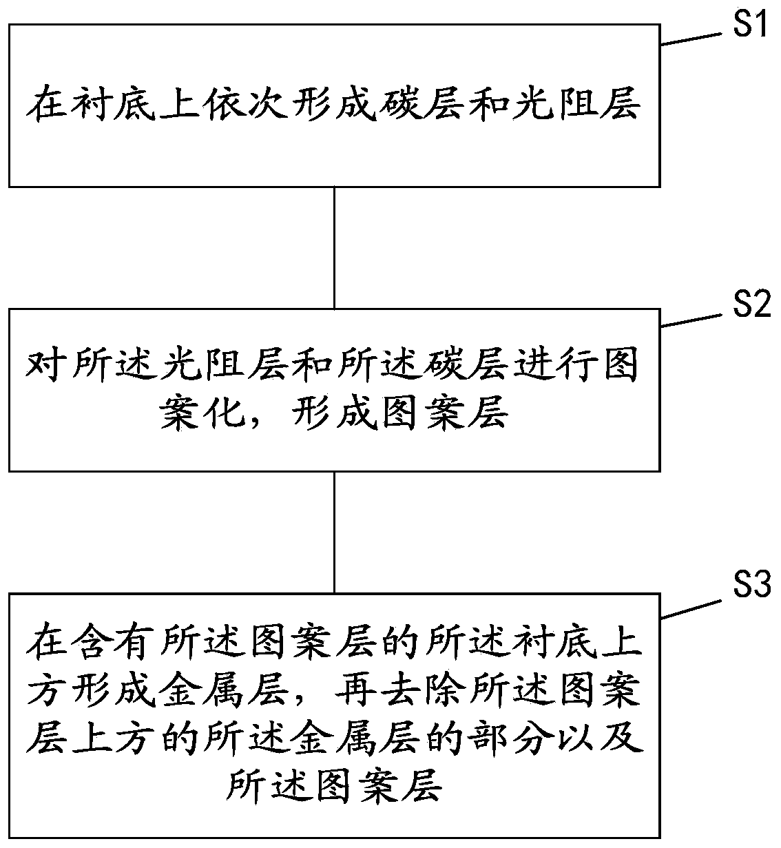
[0055] see figure 1 , the present embodiment provides a method for preparing an interdigitated electrode, comprising the following steps:
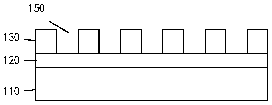
[0056] S1: see figure 2 , forming a carbon layer 120 and a photoresist layer 130 sequentially on the substrate 110 .
[0057] Wherein, the substrate 110 is made of lithium niobate or lithium tantalate. The carbon layer 120 may be formed on the substrate 110 by sputtering at a temperature below 100 degrees Celsius. The thickness of the carbon layer 120 is not less than the thickness of the required metal wire, preferably 300-3000.
[0058] S2: see Figure 3 to Figure 5 , patterning the photoresist layer 130 and the carbon layer 120 to form a patterned layer 180 .
[0059] Specifically, firstly, the photoresist layer 130 is exposed and developed to form a plurality of spaced hollow areas 150 on the photoresist layer 130 . The width of the hollow area 150 is equal to the line width of the required metal line 170 . The bottom of the ho...
no. 2 example
[0071] see Image 6 , the present embodiment provides a method for preparing an interdigitated electrode, comprising the following steps:
[0072] S21: See Figure 7 , forming the metal layer 140 on the substrate 110 .
[0073] Wherein, the metal layer 140 is a preliminary material for forming the required metal wire 170, and the thickness of the metal layer 140 is equal to the thickness of the required metal wire 170. The metal layer 140 can be made of aluminum and formed by evaporation.
[0074] S22: sequentially forming a carbon layer 120 and a photoresist layer 130 on the metal layer 140 .
[0075] Wherein, the carbon layer 120 is used as an anti-reflection layer, and can also improve the adhesion of the photoresist layer 130 .
[0076] S23: See Figure 8 , exposing and developing the photoresist layer 130 to form a plurality of spaced hollow areas 150 on the photoresist layer 130 .
[0077] Wherein, forming a plurality of spaced hollow areas 150 on the photoresist la...
PUM
 Abstract
Description
Claims
Application Information


