Photoresist bleaching and baking method and device

A baking device and photoresist technology, applied in the directions of light guides, optics, optical components, etc., can solve problems such as affecting production efficiency and long production distance, and achieve the effects of improving production efficiency, improving adaptability, and reducing equipment procurement costs.

Pending Publication Date: 2020-06-30
TCL CHINA STAR OPTOELECTRONICS TECH CO LTD
View PDF5 Cites 0 Cited by
  • Summary
  • Abstract
  • Description
  • Claims
  • Application Information

AI Technical Summary

Problems solved by technology

[0005] The production lead time of the above process is long, which affects the improvement of

Method used


Image

  • Photoresist bleaching and baking method and device
  • Photoresist bleaching and baking method and device
  • Photoresist bleaching and baking method and device

Examples


Embodiment Construction

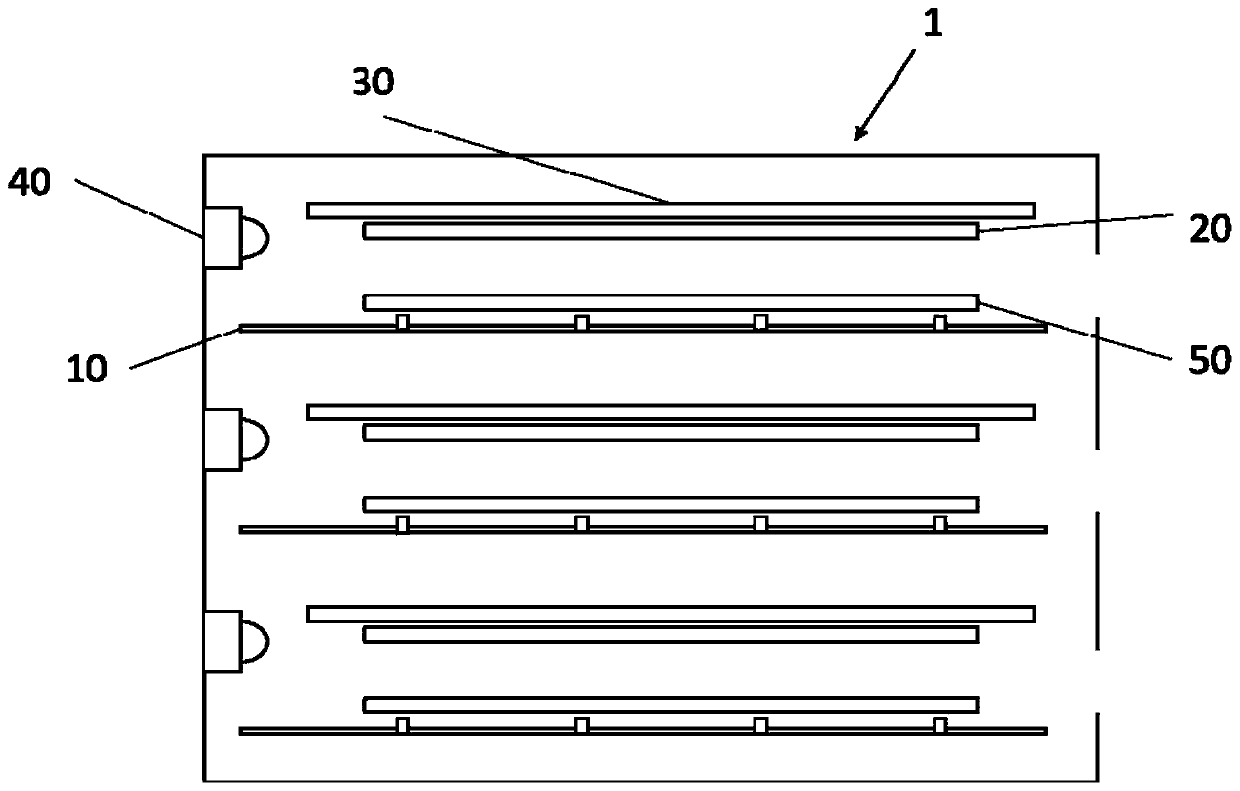
[0022] In one embodiment, a photoresist bleaching and baking device, such as figure 1 As shown, an oven 1 is included, and the oven 1 includes a plurality of heat-pressed board layers 10, a plurality of light guide plates 20, and the plurality of light guide plates 20 are arranged in the oven 1, and a plurality of reflective plates 30, the A plurality of reflective plates 30 are disposed on one side of the plurality of light guide plates 20 and are parallel to the light guide plates 30 , and a plurality of light sources 40 are disposed on the side wall inside the oven 1 .

[0023] Wherein, the plurality of light sources 40 project light on the plurality of light guide plates 20 for a period of time to perform a bleaching process, and at the same time, the plurality of hot-pressed plate layers 10 perform a hot air baking process.

[0024] In one embodiment, as figure 2 with image 3 As shown, the oven 1 includes at least one substrate 50. The substrate 50 forms a photoresist...


PUM

PropertyMeasurementUnit
Thicknessaaaaaaaaaa

Abstract

The invention discloses a photoresist bleaching and baking device and a method thereof. The device is characterized in that the device comprises an oven, the oven comprises a plurality of hot pressingplate layers, multiple light guide plates arranged in the oven, multiple reflectors which are arranged on sides of the plurality of light guide plates and are parallel to the light guide plates, anda plurality of light sources which are arranged on a side wall in the oven, wherein the plurality of light sources project a light ray to the plurality of light guide plates within a bleaching time, the light ray is uniformly distributed by lattice points of the plurality of light guide plates so as to carry out a bleaching process, and meanwhile, the plurality of hot pressing plate layers are subjected to a hot air baking process.

Description

【Technical field】 [0001] The disclosure relates to the field of display technology, in particular to a photoresist bleaching and baking method and device thereof. 【Background technique】 [0002] In semiconductor display devices such as thin-film liquid crystal displays and organic light-emitting diodes, a passivation layer (PV) is generally used for insulation, passivation, and planarization, and its film quality includes SiNx and SiOx. With the continuous improvement of the market's demand for device performance, the technology of polyimide film on array (Polymer Film on Array, PFA) has gradually been widely used. ) process uses acrylic resin to replace the original PV2 film layer, and replaces the original chemical vapor deposition (Chemical Vapor Deposition, CVD), yellow light, and etching process with the process of coating photoresist film layer, which has the advantages of reducing parasitic capacitance, There are many advantages such as increasing the aperture ratio ...

Claims


Application Information

Patent Timeline
IPC IPC(8): G03F7/40G02B6/00
CPCG03F7/40G02B6/0055
Inventor 高攀
Owner TCL CHINA STAR OPTOELECTRONICS TECH CO LTD
Why Eureka
Try Eureka