Silicon bar cutting technology

A cutting process and silicon rod technology, which is applied in the direction of manufacturing tools, stone processing equipment, fine working devices, etc., can solve the problems of increasing the difficulty and cost of the silicon rod process and the limitation of the length and width of silicon wafers, so as to reduce production costs, The effect of improving the utilization rate

Active Publication Date: 2020-07-03
CHANGZHOU SHICHUANG ENERGY CO LTD
View PDF5 Cites 5 Cited by
  • Summary
  • Abstract
  • Description
  • Claims
  • Application Information

AI Technical Summary

Problems solved by technology

[0003] The overall shape of the silicon wafer is generally rectangular, but in the existing silicon rod cutting process, the slicing direction is perpendicular to the extending direction of the silicon block, that is, the slicing direction is perpendicular to the extending direction of the silicon rod, so the length and width of the silicon wafer are all affected by the silicon rod. diameter limit
If a rectangular silicon wafer with a larger length and size is to be prepared, a silicon rod with a larger diameter must be prepared in advance, which increases the difficulty and cost of the silicon rod preparation process

Method used


Image

  • Silicon bar cutting technology
  • Silicon bar cutting technology
  • Silicon bar cutting technology

Examples


Embodiment Construction

[0024] The specific implementation manners of the present invention will be further described below in conjunction with the drawings and examples. The following examples are only used to illustrate the technical solution of the present invention more clearly, but not to limit the protection scope of the present invention.

[0025] The technical scheme of concrete implementation of the present invention is:

[0026] like Figure 1 to Figure 3 Shown, the present invention provides a kind of silicon rod cutting process, comprises the steps:

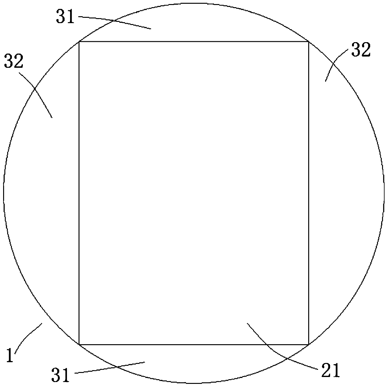
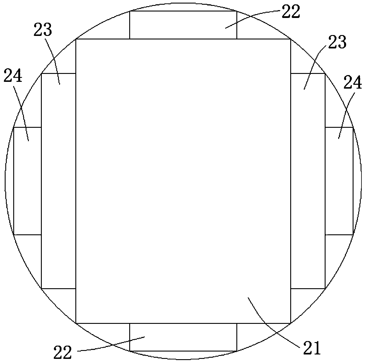
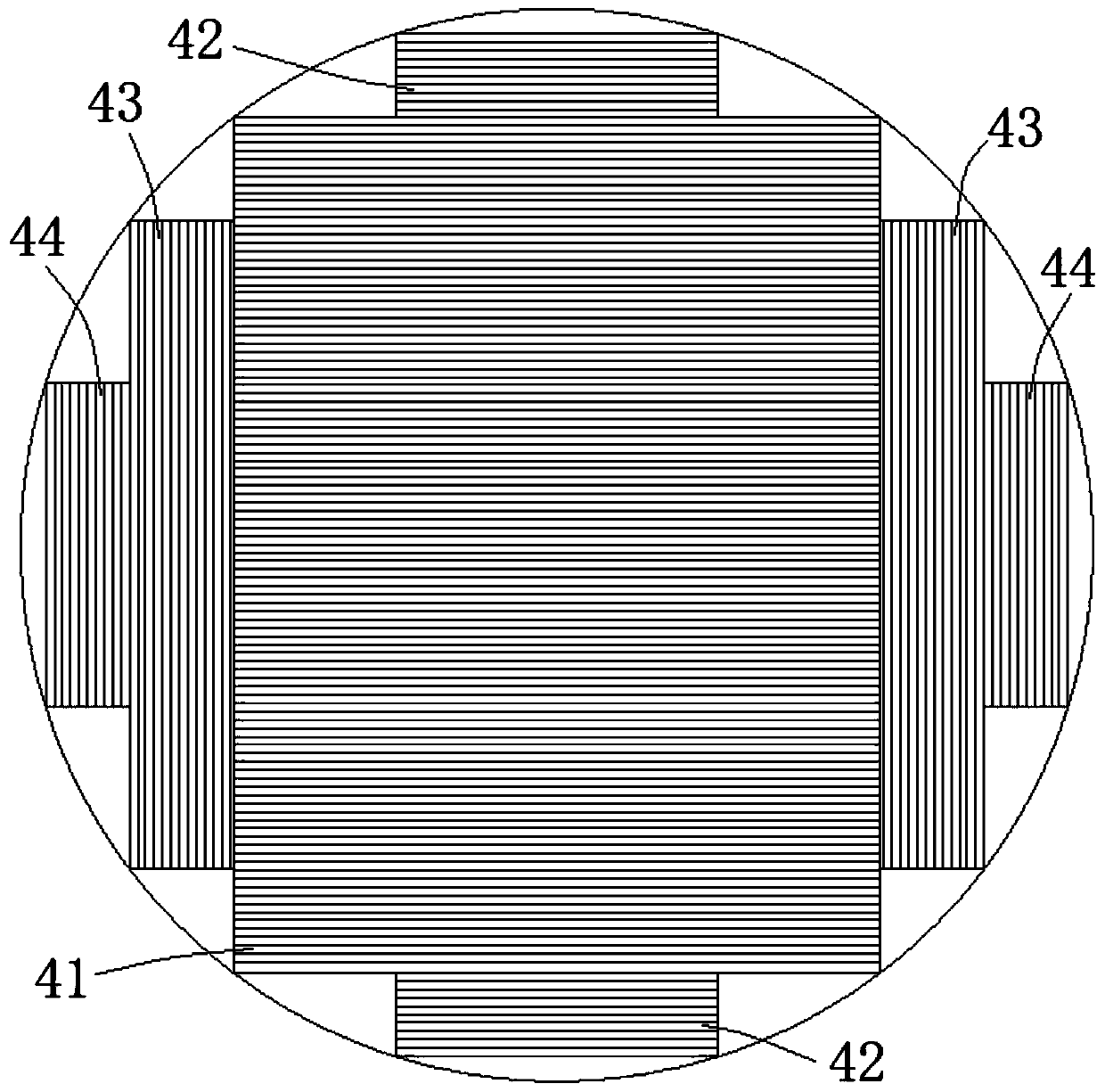
[0027] The square of the silicon rod 1 is cut out to extend in the same direction as the silicon rod 1: a central silicon block 21 and four side leather materials; the cross section of the central silicon block 21 is rectangular, and the cross section of the central silicon block 21 is the same as the silicon rod 1 The direction of extension is vertical; the four side leather materials include: a pair of first side leather materials 31 cut ...


PUM

PropertyMeasurementUnit
lengthaaaaaaaaaa
widthaaaaaaaaaa
widthaaaaaaaaaa

Abstract

The invention discloses a silicon bar cutting technology. The silicon bar cutting technology comprises the following steps that firstly, silicon bar square forming is conducted, and a center silicon block and four edge materials which extend in the same direction with a silicon bar are cut; the four edge materials are cut into a first small silicon block, a second small silicon block and a third small silicon block which extend in the same direction with the silicon bar; the length of the cross sections of the first small silicon block and the third small silicon block is 1 / 2 of the width of the cross section of the center silicon block; the length of the cross section of the second small silicon block is the same with the width of the cross section of the center silicon block; and slicingis conducted on the center silicon block, the first small silicon block, the second small silicon block and the third small silicon block, and the slicing direction is parallel to the silicon bar extending direction. The slicing direction is parallel to the silicon bar extending direction, and therefore the length size of a silicon wafer obtained through slicing cannot be limited by the diameterof the silicon bar, and a rectangular silicon wafer with the large length size is easily prepared; and by means of the silicon bar cutting technology, two kinds of silicon wafers different in width specification can be cut, the silicon bar utilization rate can be increased, and the silicon wafer production cost is reduced.

Description

technical field [0001] The invention relates to a silicon rod cutting process. Background technique [0002] Monocrystalline silicon wafers for solar cells are generally cut from silicon rods. Specifically, silicon rods (ie, round rods) are generally squared first, and silicon blocks (ie, square rods or quasi-square rods) are cut out, and then the silicon blocks are sliced ​​to produce silicon wafers. [0003] The overall shape of the silicon wafer is generally rectangular, but in the existing silicon rod cutting process, the slicing direction is perpendicular to the extending direction of the silicon block, that is, the slicing direction is perpendicular to the extending direction of the silicon rod, so the length and width of the silicon wafer are all affected by the silicon rod. diameter limitation. If a rectangular silicon wafer with a larger length and size is to be prepared, a silicon rod with a larger diameter must be prepared in advance, which increases the difficu...

Claims


Application Information

Patent Timeline
Patent Type & Authority Applications(China)
IPC IPC(8): B28D5/00H01L21/02
CPCB28D5/00H01L21/02005Y02P70/50
Inventor 曹育红岳维维符黎明
Owner CHANGZHOU SHICHUANG ENERGY CO LTD
Why Eureka
Try Eureka