Thermal budget automatic control method and automatic control system thereof
An automatic control system and thermal budget technology, applied in semiconductor/solid-state device manufacturing, electrical components, semiconductor/solid-state device testing/measurement, etc. Problems such as dynamic adjustment of different silicon wafers
- Summary
- Abstract
- Description
- Claims
- Application Information
AI Technical Summary
Problems solved by technology
Method used
Image
Examples
no. 1 example
[0047] In the first embodiment, the present invention provides a thermal budget automatic control method for rapid thermal annealing SMT RTA process of integrated circuit stress memory technology, including the following steps:
[0048] S1, according to the process requirements, set the target value of the side wall thickness, the qualified range of the side wall thickness and the thermal budget tolerance range of the side wall thickness;
[0049] Among them, the thermal budget tolerance interval of the side wall thickness is a non-empty subset of the qualified interval of the side wall thickness.
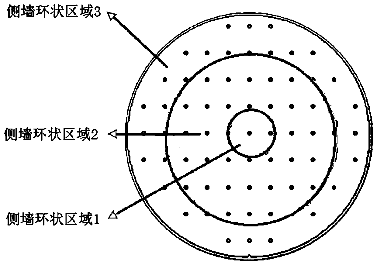
[0050] S2, measuring the thickness value of the entire side wall of the silicon wafer, calculating the average value of the thickness of the inner side wall of the chip and the deviation between the thickness value of the inner side wall in the ring-shaped area of the different side wall and the target value of the side wall thickness; the deviation refers to the measured value an...
no. 2 example
[0057] In the second embodiment, the present invention provides a thermal budget automatic control method for rapid thermal annealing SMT RTA process of integrated circuit stress memory technology, comprising the following steps:
[0058] S1, according to the process requirements, set the target value of the side wall thickness, the qualified range of the side wall thickness and the thermal budget tolerance range of the side wall thickness;
[0059] Side wall thickness target value is range is The qualified range of side wall thickness is The thermal budget tolerance range of side wall thickness is
[0060] in, And b>a, X>Y≥1.
[0061] Optionally, the target value of side wall thickness is the target value of optical measurement; hypothetically, the target value of optical measurement of side wall thickness Then the qualified range of side wall thickness is The thermal budget tolerance range of side wall thickness is
[0062] S2, measuring the thickness valu...
no. 3 example
[0069] In the third embodiment, the present invention provides a thermal budget automatic control system for rapid thermal annealing SMT RTA process of integrated circuit stress memory technology, including:
[0070] Standard setting module, which is suitable for setting the target value of side wall thickness, the qualified range of side wall thickness and the thermal budget tolerance range of side wall thickness according to the process requirements;
[0071] Among them, the thermal budget tolerance interval of the side wall thickness set by the standard setting module is a non-empty subset of the qualified interval of the side wall thickness;
[0072] The measurement and calculation module is suitable for measuring the thickness of the entire side wall of the silicon wafer, calculating the average thickness of the inner wall of the wafer and the deviation between the thickness of the inner wall of different side wall annular regions and the target value of the side wall thic...
PUM
 Abstract
Description
Claims
Application Information


