N-polarity nitride template, N-polarity nitride device and preparation method of N-polarity nitride device
A nitride and nitride layer technology, applied in semiconductor devices, electrical components, circuits, etc., can solve the problems of poor material quality and partial polarity reversal of N-polar nitride materials
- Summary
- Abstract
- Description
- Claims
- Application Information
AI Technical Summary
Problems solved by technology
Method used
Image
Examples
preparation example Construction
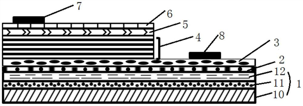
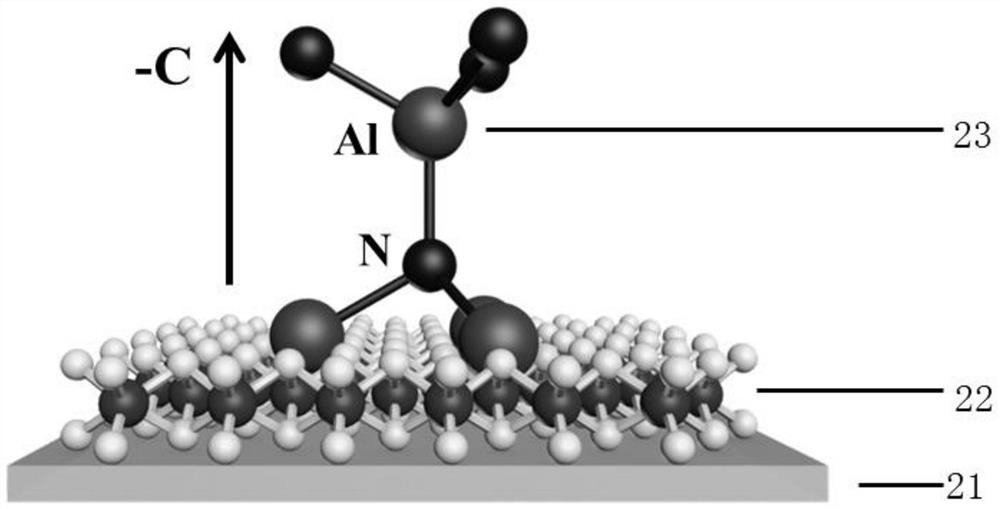
[0053] The embodiment of the present application also provides a method for preparing the above-mentioned N-polar nitride template, including the following steps:
[0054] S1. A substrate is provided, and the substrate is ultrasonically cleaned in acetone, ethanol and deionized water respectively, and then cleaned with N 2 Blow dry; then place the cleaned and dried substrate in a plasma cleaner to further clean the surface of the substrate and set aside;
[0055] S2. Prepare a transition metal oxide on the surface of the substrate. The specific preparation method is: prepare the transition metal oxide material on the surface of the substrate by powder thermal evaporation or solution spin coating, which can be controlled by thermal evaporation or Spin-coating process parameters to achieve transition metal oxide films with different thicknesses;
[0056] S3. Sulfurize the transition metal oxide to obtain a transition metal dichalcogenide. Specifically, place the substrate prepa...
Embodiment 1
[0089] A method for preparing an N-polar nitride device, comprising the following steps:
[0090] A1. Place a 2-inch sapphire substrate in acetone, ethanol, and deionized water for 5 minutes, respectively, and ultrasonically clean it with N 2 Dry the surface of the sapphire substrate with an air gun, and then dry it in a blast drying oven at 120°C for 10 minutes to remove residual moisture on the surface; place the dried sapphire substrate in a plasma cleaning machine, and feed O with a flow rate of 50 sccm. 2 , glow treatment at 50% power for 5 minutes to further clean the surface of the sapphire substrate;
[0091] A2. Deposit 2nm MoO on the surface of sapphire substrate by vacuum thermal evaporation 3 , annealed at 200°C for 30 minutes in the atmosphere to make the MoO on the sapphire substrate 3 The film can be fully oxidized and denser; the annealed sapphire MoO 3 Place the S powder in the low-pressure chemical vapor deposition equipment with dual temperature zones, pl...
PUM
 Abstract
Description
Claims
Application Information


