Testing device and testing method of IGBT device and electronic equipment

A technology of a testing device and a testing method, which is applied in the testing, measuring device, measuring electricity and other directions of a single semiconductor device, can solve the problems of difficulty in testing contact resistance, complicated measurement, etc., so as to avoid multiple testing errors, accurate testing results, and simple testing. Effect

Inactive Publication Date: 2020-07-17
GLOBAL ENERGY INTERCONNECTION RES INST CO LTD +2
View PDF0 Cites 2 Cited by
  • Summary
  • Abstract
  • Description
  • Claims
  • Application Information

AI Technical Summary

Problems solved by technology

[0008] In view of this, an embodiment of the present invention provides a test device, a test method and electronic...

Method used


Image

  • Testing device and testing method of IGBT device and electronic equipment
  • Testing device and testing method of IGBT device and electronic equipment
  • Testing device and testing method of IGBT device and electronic equipment

Examples


Embodiment Construction

[0045] In order to make the purpose, technical solutions and advantages of the embodiments of the present invention clearer, the technical solutions in the embodiments of the present invention will be clearly and completely described below in conjunction with the drawings in the embodiments of the present invention. Obviously, the described embodiments It is a part of embodiments of the present invention, but not all embodiments. Based on the embodiments of the present invention, all other embodiments obtained by those skilled in the art without creative efforts fall within the protection scope of the present invention.

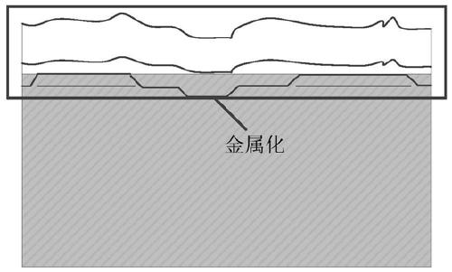
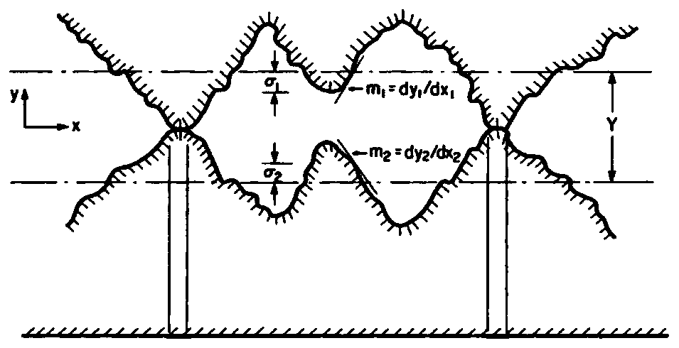
[0046] The calculation of the contact resistance of traditional IGBT devices usually needs to measure the equivalent root-mean-square surface roughness of the pressure contact surface, the equivalent average absolute surface slope, the harmonic mean of the thermal conductivity of the contact interface, and the relative softness of the two contact materials. M...


PUM


Abstract

The invention relates to the technical field of semiconductors, and in particular relates to an IGBT device testing device and method and electronic equipment. The testing device comprises a pressuresensor which is used for detecting a plurality of groups of contact pressure values applied to a to-be-tested IGBT device, and a voltmeter. Two ends of the voltmeter are respectively connected with the collector and the emitter of the IGBT device to be tested, and the voltmeter is used for detecting a plurality of groups of on-state voltage drop values between the collector and the emitter of theIGBT device to be tested. The testing device further comprises a fixed current source which is connected with the collector and the emitter of the IGBT device to be tested and is used for providing fixed current for the IGBT device to be tested, and a processor which is connected with the pressure sensor and the voltmeter and is used for calculating the contact resistance value of the IGBT deviceto be tested by utilizing the plurality of groups of contact pressure values, the plurality of groups of on-state voltage drop values, the fixed current and the pressure applying area. According to the testing device of the IGBT device, the contact resistance value is obtained through calculation by means of the multiple sets of on-state voltage drop values, the fixed current and the pressure applying area; microcosmic parameters of the IGBT device do not need to be measured; and testing is simple and easy to operate.

Description

technical field [0001] The invention relates to the technical field of semiconductors, in particular to a test device, a test method and electronic equipment for an IGBT device. Background technique [0002] Compression-type insulated gate bipolar transistor (Insulated Gate Bipolar Transistor, IGBT) is the core device of flexible direct current transmission equipment. The crimp-type IGBT device directly contacts the conductive metal electrode with the collector and emitter of the device through mechanical pressure, thereby eliminating the bonding wire in the package structure, and has low parasitic inductance, compact structure, failure short circuit, and double-sided heat dissipation And other advantages, so it is especially suitable for power system equipment applications. [0003] Due to the characteristics of the packaging structure of the crimp-type IGBT device, each device needs to bear certain mechanical stress to maintain good electrical contact. However, due to th...

Claims


Application Information

Patent Timeline
IPC IPC(8): G01R31/26
CPCG01R31/2601Y02E10/50
Inventor 张西子张喆吴军民唐新灵林仲康王亮石浩韩荣刚杜玉杰孙帅
Owner GLOBAL ENERGY INTERCONNECTION RES INST CO LTD
Why Eureka
Try Eureka