A dark current correction method for cmos image sensor

A dark current correction, image sensor technology, applied in the field of image processing, can solve the problems of chip process deviation, chip circuit power consumption difference, etc., to achieve the effect of high correction accuracy and excellent image effect

Active Publication Date: 2021-05-25
CHENGDU LIGHT COLLECTOR TECH
View PDF10 Cites 0 Cited by
  • Summary
  • Abstract
  • Description
  • Claims
  • Application Information

AI Technical Summary

Problems solved by technology

Due to the deviation of the chip process, or the power consumption of the circuits around the chip is different

Method used


Image

  • A dark current correction method for cmos image sensor
  • A dark current correction method for cmos image sensor
  • A dark current correction method for cmos image sensor

Examples


Embodiment Construction

[0031] In order to make the purpose, technical solution and advantages of the present invention clearer, the specific implementation manners of the present invention will be further described in detail below in conjunction with the accompanying drawings.

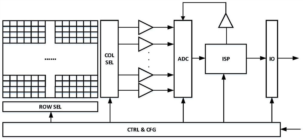
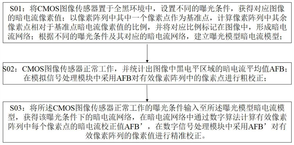
[0032] as attached image 3 As shown, a dark current correction method for a CMOS image sensor provided by the present invention is characterized in that it includes the following steps:

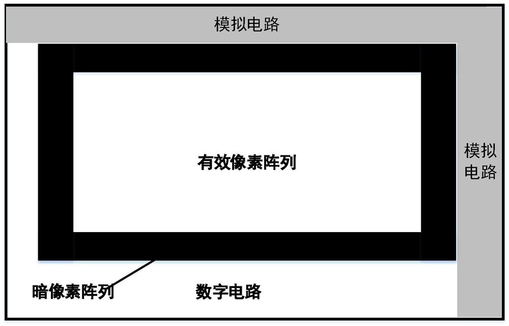
[0033] S01: Place the CMOS image sensor in a completely dark environment, set different exposure conditions, and obtain the dark current pixel value of the corresponding image; use one of the pixels in the pixel array as a reference point, and calculate the relative value of the remaining pixels in the pixel array relative to the reference point Point the ratio of the dark current pixel value, and mark the corresponding ratio in the image to form a dark current network; according to different exposure conditions and their corresponding dar...


PUM


Abstract

The invention discloses a dark current correction method of a CMOS image sensor, comprising the following steps: S01: placing the CMOS image sensor in a completely dark environment, setting different exposure conditions, and obtaining the dark current pixel value of the corresponding image; One of the pixels in the pixel array is used as a reference point, and the ratio of the remaining pixels in the pixel array to the reference point dark current pixel value is calculated, and the corresponding ratio is marked in the image to form a dark current network; S02: In the analog signal processing module, use AFB roughly corrects the pixels in the effective pixel array; S03: Calculate the dark current correction value AFB' of each pixel in the effective pixel array through a digital algorithm in the dark current network, and use AFB' in the digital signal processing module to correct The pixel values ​​of the active pixel array are precisely corrected. The method for correcting dark current of a CMOS image sensor provided by the present invention has high precision for dark current correction, and the correction result is more in line with actual application conditions.

Description

technical field [0001] The invention relates to the field of image processing, in particular to a dark current correction method of a CMOS image sensor. Background technique [0002] In the process of image processing, the image collected by the CCD / CMOS image sensor is usually processed. However, when a CMOS image sensor is used to collect images, even if the pixels of the image sensor manufactured by the CMOS process are not exposed, the output of the ADC is not zero due to the existence of dark current, resulting in an image that does not appear absolutely black in the case of complete shading. . The output level of the image sensor in a completely dark environment is called dark current. Dark current will affect the color reproduction, dynamic range and clarity of the image and needs to be corrected to eliminate it. [0003] The magnitude of the dark current has a linear relationship with the exposure time and an exponential relationship with the temperature. Every t...

Claims


Application Information

Patent Timeline
Patent Type & Authority Patents(China)
IPC IPC(8): H04N5/217H04N5/374H04N5/361H04N5/369
CPCH04N25/63H04N25/633H04N25/76
Inventor 宋博喻义淞温建新王勇
Owner CHENGDU LIGHT COLLECTOR TECH
Why Eureka
Try Eureka