Supercharge Your Innovation With Domain-Expert AI Agents!

Magnetic shielding structure for mram array

A cell array, metal structure technology, applied in the field of magnetic shielding

Pending Publication Date: 2020-07-21
NXP BV
View PDF0 Cites 1 Cited by
  • Summary
  • Abstract
  • Description
  • Claims
  • Application Information

AI Technical Summary

Problems solved by technology

Although MRAM technology is relatively new, said technology has significant application opportunities

Method used


Image

  • Magnetic shielding structure for mram array
  • Magnetic shielding structure for mram array
  • Magnetic shielding structure for mram array

Examples


Embodiment Construction

[0034] A detailed description of various embodiments intended to illustrate the invention is set forth below and should not be considered limiting.

[0035] overview

[0036] Typically, a magnetoresistive random access memory (MRAM) includes a large number of magnetic bit cells formed on a semiconductor substrate, where each cell represents a data bit. Information is written to a bit cell by changing the magnetization direction of a magnetic element within the bit cell, and the bit cell is read by measuring the resistance of the bit cell (e.g., a low resistance typically represents a "0" bit and a high resistance typically represents a "1" bits). Bit cells are programmed using programming lines, commonly referred to as bit lines and digit (or word) lines.

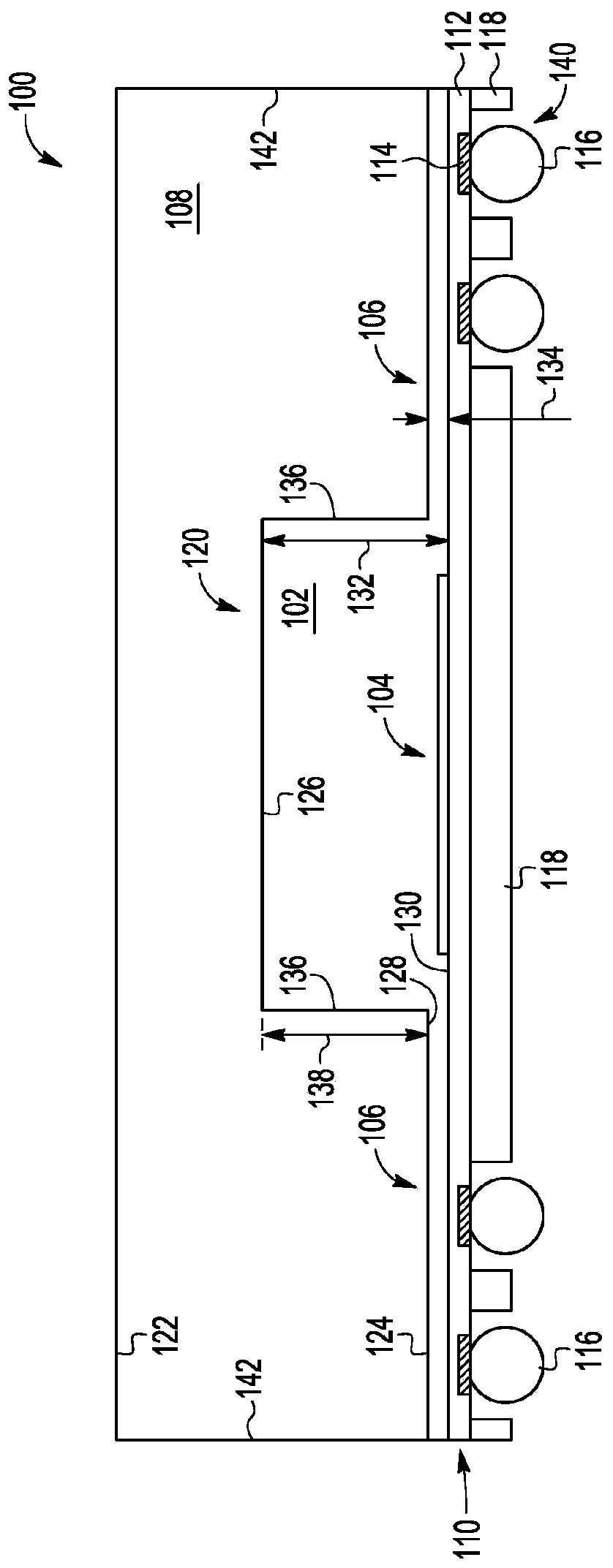
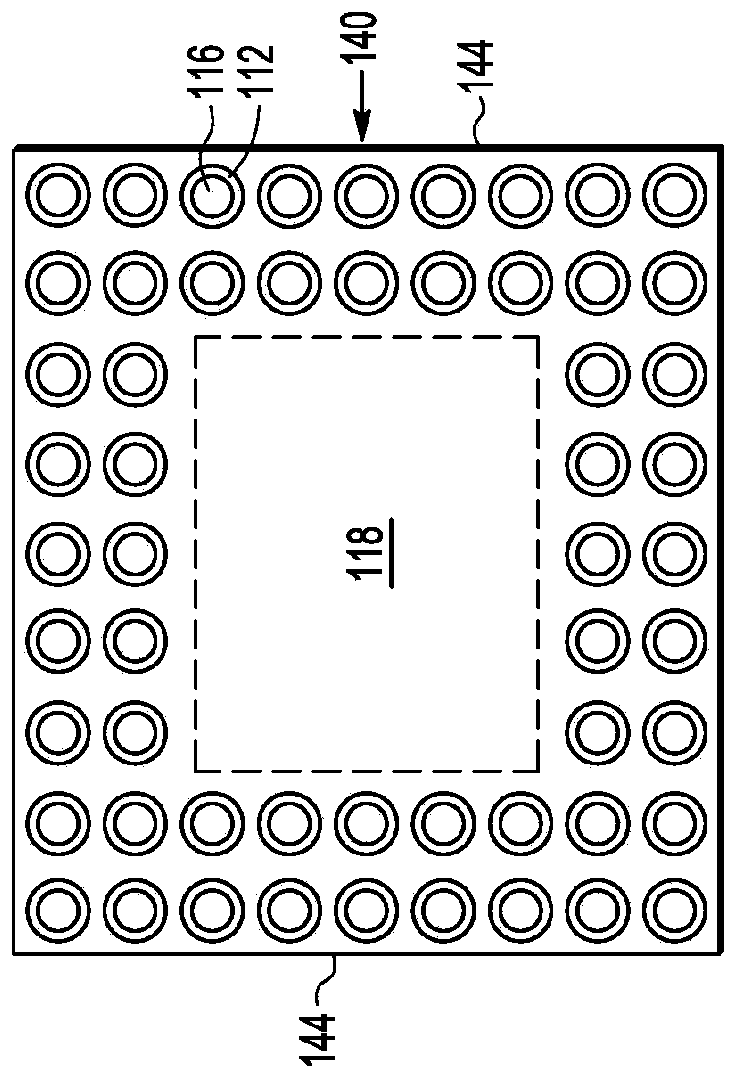
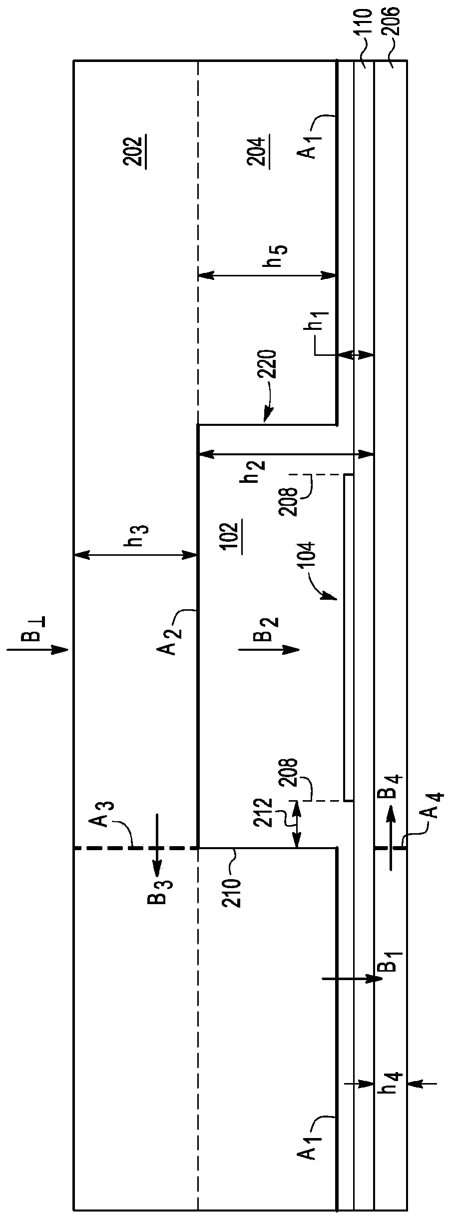
[0037]One disadvantage of memory arrays implemented using MRAM cells is the lack of immunity to magnetic fields in the surrounding environment, which can disturb or corrupt data values ​​stored by multiple magnetic bit ...


PUM


Abstract

Embodiments are provided for a packaged semiconductor device including: a semiconductor die having an active side and an opposite back side, the semiconductor die including a magnetoresistive random access memory (MRAM) cell array formed within an MRAM area on the active side of the semiconductor die; and a top cover including a soft- magnetic material positioned on the back side of the semiconductor die, wherein the top cover includes a recess formed in a first major surface of the top cover, the first major surface faces the back side of the semiconductor die, and the recess is positioned over the MRAM cell array.

Description

technical field [0001] The present disclosure relates generally to magnetoresistive random access memory (MRAM) systems, and more particularly, to magnetic shielding for MRAM. Background technique [0002] MRAM is a memory technology that uses magnetic polarization to store data, in contrast to Random Access Memory (RAM) technology that uses electrical charges to store data. A major benefit of MRAM is that it retains stored data when system power is not applied, making it a non-volatile memory suitable for implementation in a variety of devices. Although MRAM technology is relatively new, the technology has significant application opportunities. Contents of the invention [0003] In one embodiment of the present disclosure, a packaged semiconductor device is provided that includes a semiconductor die having an active side and an opposite backside, the semiconductor die including a magnetic an array of resistive random access memory (MRAM) cells formed within the MRAM reg...

Claims


Application Information

Patent Timeline
Patent Type & Authority Applications(China)
IPC IPC(8): H01L43/08H01L43/02H01L43/12H01L27/22H01L23/552
CPCH01L23/552H10B61/00H10N50/80H10N50/01H10N50/10
Inventor 弗朗西斯科斯·皮特鲁斯·韦德索文安托尼斯·亨德里库斯·尤立夫·坎菲斯
Owner NXP BV
Features
  • R&D
  • Intellectual Property
  • Life Sciences
  • Materials
  • Tech Scout
  • Unparalleled Data Quality
  • Higher Quality Content
  • 60% Fewer Hallucinations
Learn More