

System-in-package method and structure of heterogeneous integrated chip
A system-level packaging and integrated chip technology, which is applied in the manufacture of electrical components, electrical solid devices, semiconductor/solid devices, etc., can solve the problems that heterogeneous chips cannot be integrated and packaged, so as to reduce process costs, reduce costs, and reduce process difficulty Effect
- Summary
- Abstract
- Description
- Claims
- Application Information
AI Technical Summary
Problems solved by technology
Method used
Image

Examples
Embodiment 1
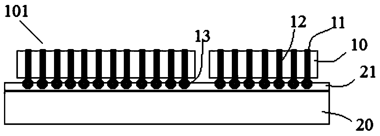
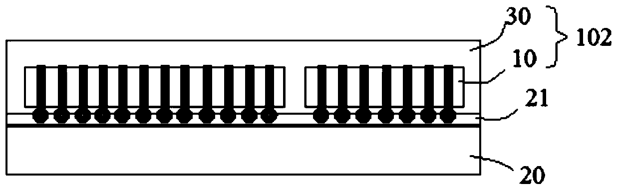
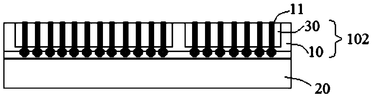
[0048] This embodiment provides a system-in-package method for heterogeneous integrated chips, such as Figure 1-10 As shown, the system-in-package method of the heterogeneous integrated chip includes: making a plurality of silicon substrate chips 10; a plurality of the silicon substrate chips 10 facing away from a carrier 20 and sticking them together on the carrier 20, Form the first integrated adapter plate 101; as figure 2 As shown, a first plastic packaging layer 30 is formed on the first integrated interposer 101, and the silicon substrate chip 10 and the first plastic packaging layer 30 form a first plastic packaging body 102; image 3 As shown, the top of the first plastic package 102 is mechanically or chemically polished, exposing a plurality of electrical leads 11 of the silicon substrate chips 10; Figure 4 As shown, a metal interconnection layer and a dielectric layer 40 are made on top of a plurality of silicon substrate chips 10, and the metal interconnection l...
Embodiment 2
[0060] This embodiment also provides a system-in-package structure of a heterogeneous integrated chip, such as Figure 7 As shown, it includes: a plurality of silicon substrate chips 10; a first plastic sealing layer 30, and the first plastic sealing layer 30 covers the top of the silicon substrate chips 10 and the carrier 20; a plurality of silicon substrate chips 10 The electrical lead-out part 11 is exposed on the top of the first plastic encapsulation layer 30; the metal interconnection layer and the dielectric layer 40 are located on the top of the first plastic encapsulation layer 30, and the metal interconnection layer and the plurality of silicon substrates The electrical lead-out part 11 of the chip 10 is electrically connected; a plurality of heterogeneous chips 50 are located on the top of the metal interconnection layer and the dielectric layer 40 and are electrically connected with the metal interconnection layer and the dielectric layer 40. The heterogeneous chips...
PUM
| Property | Measurement | Unit |
|---|---|---|
| Thickness | aaaaa | aaaaa |
| Thickness | aaaaa | aaaaa |
Abstract
Description
Claims
Application Information