Manufacturing method of wafer-level glass cavity

A manufacturing method and wafer-level technology, applied in the manufacture of microstructure devices, techniques for producing decorative surface effects, decorative arts, etc., can solve the problem that it is difficult to obtain cavities with a depth greater than 50um, and the back of a glass sheet cannot be obtained very well. Good protection, depth cannot be precisely controlled, etc., to achieve the effect of eliminating surface undercutting, reducing defects and pinholes, and low cost

Pending Publication Date: 2020-08-07
BEIJING INST OF AEROSPACE CONTROL DEVICES
View PDF16 Cites 0 Cited by
  • Summary
  • Abstract
  • Description
  • Claims
  • Application Information

AI Technical Summary

Problems solved by technology

In the wet etching process, the traditional method is to select a single type of mask, and the back of the glass sheet cannot be well protected, resulting in serious undercutting of the glass sheet during the etching process, and it is difficult to obtain a cavity with a depth greater than 50um. body
If the DRIE method is used to etch the cavity with SF6 gas, the etching efficiency is low and the depth cannot be precisely controlled
Invention patent application "Manufacturing method of wafer-level glass microcavity" (application number 200810023417.4) and invention patent application "Manufacturing method of MEMS packaged glass microcavity with optical window" (application number 200910185356.6) proposed to use silicon dry etching, The method of softening the glass after anodic bonding is used to make the glass deep cavity. Although this method can obtain a pattern with an aspect ratio of 20:1, when the depth exceeds 100 μm, the deviation in the chip is large, and the production efficiency is low.

Method used


Image

  • Manufacturing method of wafer-level glass cavity
  • Manufacturing method of wafer-level glass cavity
  • Manufacturing method of wafer-level glass cavity

Examples


Embodiment 1

[0043] In the first step, the Pyrex7740 glass slides were successively soaked with 120°C 3# solution (H 2 SO 4 :H 2 o 2 =4:1) Wash for 20min, 1# solution (NH 4 OH:H 2 o 2 :H 2 O=1:1:5) wash for 20min, 2# solution (HCl: H 2 o 2 :H 2 O=1:1:6) Wash for 20 minutes, rinse with water, and shake dry.

[0044] In the second step, put the glass sheet in 60°C, 20% KOH solution for cleaning for 10 minutes, rinse with water, and spin dry.

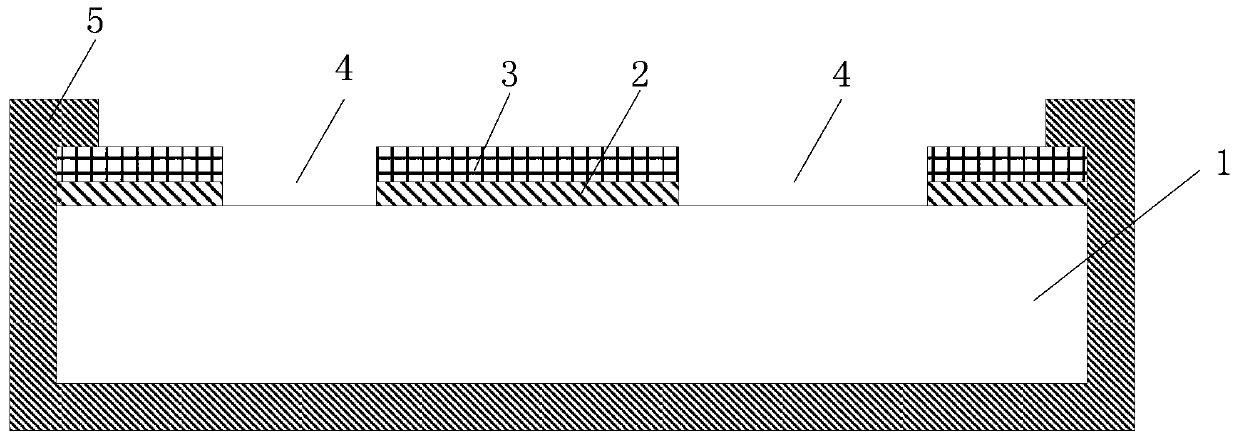
[0045] In the third step, a Cr / Au film with a thickness of 40nm / 200nm is deposited on one side of the glass sheet by using a magnetron sputtering station.

[0046] The fourth step is to apply i7010 photoresist on the metal surface of the glass sheet with a thickness of 2 μm, and use photolithography and dry etching to form a specific pattern on the Cr / Au film and expose the glass surface.

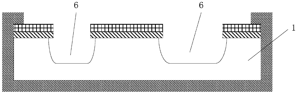
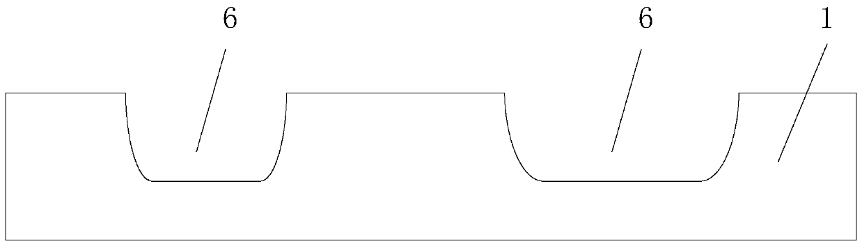
[0047] The fifth step is to use SPV225 blue film (thickness 80μm). Airtightly bond the edge of the glass sheet and the surface without the gold film.

...

Embodiment 2

[0051]In the first step, the TEMPAX glass sheets were successively soaked with 120°C 3# liquid (H 2 SO 4 :H 2 o 2 =4:1) Wash for 20min, 1# solution (NH 4 OH:H 2 o 2 :H 2 O=1:1:5) wash for 20min, 2# solution (HCl: H 2 o 2 :H 2 O=1:1:6) Wash for 20 minutes, rinse with water, and shake dry.

[0052] In the second step, put the glass sheet in 80°C, 40% KOH solution for cleaning for 20 minutes, rinse with water, and spin dry.

[0053] In the third step, a Ti / Au film with a thickness of 40nm / 400nm is deposited on one side of the glass sheet by using a magnetron sputtering station.

[0054] The fourth step is to apply 108cp photoresist on the metal surface of the glass sheet with a thickness of 5 μm, and use photolithography and dry etching to form a specific pattern on the Ti / Au film and expose the glass surface.

[0055] The fifth step is to use SPV224 blue film (thickness 80μm, adhesion force 1.10N / mm 2 ) Airtightly bond the edge of the glass sheet and the surface with...

Embodiment 3

[0059] In the first step, the TEMPAX glass sheets were successively soaked with 120°C 3# liquid (H 2 SO 4 :H 2 o 2 =4:1) Wash for 20min, 1# solution (NH 4 OH:H 2 o 2 :H 2 O=1:1:5) wash for 20min, 2# solution (HCl: H 2 o 2 :H 2 O=1:1:6) Wash for 20 minutes, rinse with water, and shake dry.

[0060] In the second step, put the glass sheet in 80°C, 40% KOH solution for cleaning for 20 minutes, rinse with water, and spin dry.

[0061] In the third step, a Ti / Au film with a thickness of 40nm / 800nm ​​is deposited on one side of the glass sheet by using a magnetron sputtering station.

[0062] The fourth step is to apply AZ4620 photoresist on the metal surface of the glass sheet with a thickness of 10 μm, and use photolithography and wet etching to form a specific pattern on the Ti / Au film and expose the glass surface.

[0063] The fifth step is to use SPV224 blue film (thickness 80μm, adhesion force 1.10N / mm 2 ) Airtightly bond the edge of the glass sheet and the surface...


PUM

PropertyMeasurementUnit
thicknessaaaaaaaaaa
thicknessaaaaaaaaaa
thicknessaaaaaaaaaa

Abstract

The invention relates to a manufacturing method of a wafer-level glass cavity. The manufacturing method comprises the following steps: cleaning a glass sheet to remove organic matters and particles onthe surface of the glass; continuously cleaning the glass sheet with a strong alkali solution, so that the OH <-> concentration of the surface of the glass sheet is increased, and the metal film adhesion is improved; sputtering a composite gold film on one surface of the glass sheet by using a metal film process; photoetching the gold film through photoetching and etching processes in sequence, and forming a specific pattern; protecting the edge of the glass sheet and the gold-free film surface by a blue film; putting the protected glass sheet into a mixed solution of HF and water, and corroding the protected glass sheet to a preset certain depth; and removing the blue film, and removing the photoresist and the composite gold film to form a cavity on the glass sheet.

Description

technical field [0001] The invention belongs to the micro-mechanical electronic MEMS manufacturing technology, in particular to a method for manufacturing a wafer-level glass cavity. Background technique [0002] In the field of MEMS manufacturing technology, glass for bonding (a glass containing alkaline ions, including Pyrex7740, TEMPAX) is an important material, because it has a thermal expansion coefficient similar to that of silicon, and can be bonded to silicon by using anodic bonding. The bottom forms a high-strength bonding connection, and the strength of the Si-O covalent bond formed on the bonding surface is even higher than that of the silicon material itself, making the bonding glass form widely used in MEMS devices, MEMS packaging, microfluidics and MOEMS and other fields. [0003] In the field of MEMS packaging, since MEMS devices generally have movable parts, it is necessary to use a cavity structure to seal and protect the device during packaging, so that the...

Claims


Application Information

Patent Timeline
Patent Type & Authority Applications(China)
IPC IPC(8): B81C1/00
CPCB81C1/00785B81C1/00539B81C1/00396B81C1/00595B81C1/00047
Inventor 杨静刘福民刘国文徐宇新梁德春
Owner BEIJING INST OF AEROSPACE CONTROL DEVICES
Why Eureka
Try Eureka