
Semi-floating gate memory based on pn junction and Schottky diode and its preparation method

A Schottky diode, semi-floating gate technology, applied in semiconductor/solid-state device manufacturing, semiconductor devices, transistors, etc., can solve the problems of small driving current, affecting the erasing and writing speed of semi-floating gate transistors, and improve the erasing speed. , The effect of improving the charge writing speed

Active Publication Date: 2022-06-21
FUDAN UNIV +1
View PDF10 Cites 0 Cited by
  • Summary
  • Abstract
  • Description
  • Claims
  • Application Information

AI Technical Summary

Problems solved by technology

However, the tunneling transistor is a minority current device, which means that the driving current of the tunneling transistor is small, which will affect the erasing speed of the semi-floating gate transistor.

Method used


Image

  • Semi-floating gate memory based on pn junction and Schottky diode and its preparation method
  • Semi-floating gate memory based on pn junction and Schottky diode and its preparation method
  • Semi-floating gate memory based on pn junction and Schottky diode and its preparation method

Examples


Embodiment Construction

[0037] In order to make the objectives, technical solutions and advantages of the present invention clearer, the technical solutions in the embodiments of the present invention will be clearly and completely described below with reference to the accompanying drawings in the embodiments of the present invention. It should be understood that the specific The embodiments are only used to explain the present invention, and are not intended to limit the present invention. The described embodiments are only some, but not all, embodiments of the present invention. Based on the embodiments of the present invention, all other embodiments obtained by those of ordinary skill in the art without creative efforts shall fall within the protection scope of the present invention.

[0038] In the description of the present invention, it should be noted that the orientation or positional relationship indicated by the terms "upper", "lower", "vertical", "horizontal", etc. is based on the orientat...


PUM


Abstract

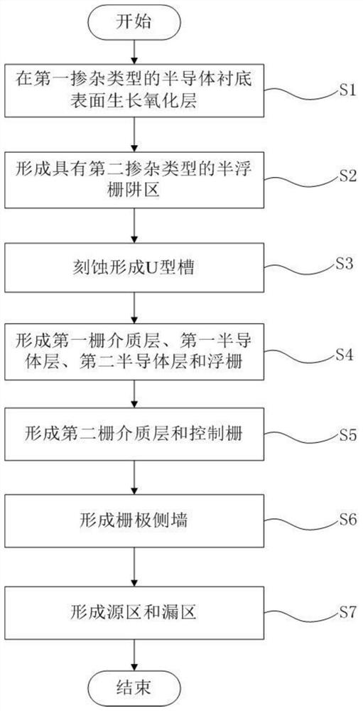
The invention belongs to the technical field of integrated circuit memory, in particular to a semi-floating gate memory based on a pn junction and a Schottky diode and a preparation method thereof. The semi-floating gate memory disclosed by the present invention is to embed a pn junction and a Schottky diode inside the floating gate transistor at the same time, as channels for charge erasing and writing respectively; The voltage is very small; using the pn junction as the channel for charge erasing can greatly increase the erasing speed; Schottky diodes also have rectification characteristics, and the turn-on voltage is also very small; using Schottky diodes as the channel for charge writing, The charge writing speed can be greatly improved.

Description

technical field [0001] The invention belongs to the technical field of integrated circuit memory, and in particular relates to a semi-floating gate memory based on a pn junction and a Schottky diode and a preparation method thereof. Background technique [0002] At present, DRAM devices used in integrated circuit chips are mainly 1T1C structures, that is, a transistor is connected in series with a capacitor, and the capacitor is charged and discharged through the switch of the transistor, thereby realizing the conversion between DRAM devices 0 and 1. As the device size becomes smaller and smaller, DRAM devices used in integrated circuit chips are facing more and more problems. For example, DRAM devices require 64 ms to refresh once, so the capacitance value of the capacitor must be kept above a certain value to ensure sufficient Long charge retention time, but as the feature size of integrated circuits shrinks, the manufacture of large capacitors has become more and more dif...

Claims


Application Information

Patent Timeline
Patent Type & Authority Patents(China)
IPC IPC(8): H01L27/108H01L21/8242H10B12/00
CPCH10B12/20H10B12/01
Inventor 朱宝陈琳孙清清张卫
Owner FUDAN UNIV
Learn More