
A method for preparing a silicon carbide jfet gate structure with rectification

A gate structure, silicon carbide technology, used in semiconductor/solid-state device manufacturing, electrical components, circuits, etc., to achieve the effect of expanding the working range, avoiding accidental opening, and improving channel conduction performance

Active Publication Date: 2017-11-21
NO 55 INST CHINA ELECTRONIC SCI & TECHNOLOGYGROUP CO LTD
View PDF5 Cites 0 Cited by
  • Summary
  • Abstract
  • Description
  • Claims
  • Application Information

AI Technical Summary

Problems solved by technology

[0005] What the present invention proposes is a kind of preparation method of silicon carbide JFET gate structure with rectification function, and its purpose is to solve the above-mentioned technical problem existing in the prior art, inject the second kind of carrier and make the device channel resistance greatly increase In the falling state, the normal operation of the device is still guaranteed, which can avoid the defect that accidental opening is easy to occur in the case of system fluctuations

Method used


Image

  • A method for preparing a silicon carbide jfet gate structure with rectification
  • A method for preparing a silicon carbide jfet gate structure with rectification
  • A method for preparing a silicon carbide jfet gate structure with rectification

Examples


Embodiment Construction

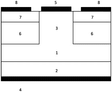
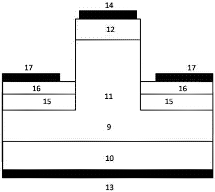
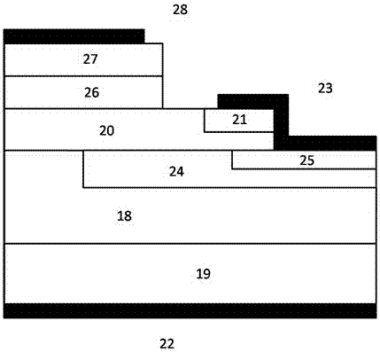
[0020] A method for preparing a silicon carbide JFET gate structure with a rectification function, comprising the following process steps:

[0021] 1) growing a first conductivity type layer 1 on a first conductivity type substrate 2;

[0022] 2) Two parts of the gate contact region 7 and the gate region 6 with the second conductivity type are respectively formed by two sets of implants, and the gate region 6 forms a PN junction with the drift region 1 and the channel region 3 with the first conductivity type;

[0023] 3) realizing ohmic contact between the source electrode 5 and the channel region 3 and between the drain electrode 4 and the substrate 2 of the first conductivity type by ohmic contact annealing;

[0024] 4) A rectifying gate contact is formed between the gate electrode 8 and the gate contact region 7 of the second conductivity type by rectifying gate contact annealing.

[0025] The turn-on voltage of the rectification grid can be controlled at 2V-20V.

[0026...


PUM


Abstract

The invention relates to a method for preparing a silicon carbide JFET gate structure with a rectification function, comprising: 1) growing a first conductivity type layer on a first conductivity type substrate; 2) forming a PN junction; 3) realizing it by ohmic annealing Source and drain ohmic contacts; 4) Rectifying gate contact is formed through rectifying gate contact annealing. Advantages: Compared with the conventional silicon carbide JFET gate structure, it has the advantages of wide controllable gate voltage range and small gate current. The gate contact region 7 is added on the basis of the conventional silicon carbide JFET structure, and the rectification characteristic is introduced between the gate electrode 8 and the gate contact region 7 by adjusting the doping concentration and annealing conditions of the gate contact region to limit the gate current and expand the gate voltage range , using the gate injection carrier induction effect to improve the channel conduction ability.

Description

technical field [0001] The invention relates to a method for preparing a silicon carbide JFET gate structure with a rectification function, and belongs to the technical field of semiconductor devices. Background technique [0002] SiC materials have large bandgap width, high breakdown electric field, high saturation drift velocity and high thermal conductivity. The superior properties of these materials make them ideal materials for making high-power, high-frequency, high-temperature-resistant, and radiation-resistant devices. SiC JFETs are of great value in high-power applications, thanks to the high stability of the junction gate, which is not limited by the reliability of the gate oxide layer in the MOS structure. [0003] One of the important reasons that currently limit the wide-scale application of SiC JFETs is the complexity of the driving circuit and system damage caused by accidental turn-on. Since the gate current of the junction gate will grow rapidly after the g...

Claims


Application Information

Patent Timeline
Patent Type & Authority Patents(China)
IPC IPC(8): H01L21/04
CPCH01L21/048H01L29/401H01L29/42316H01L29/808
Inventor 黄润华陶永洪柏松陈刚
Owner NO 55 INST CHINA ELECTRONIC SCI & TECHNOLOGYGROUP CO LTD
Learn More