Preparation and working characteristics of ZnPc/PbPc blending evaporation thin-film diode
A technology of evaporating thin films and diodes, which is applied in semiconductor/solid-state device manufacturing, organic semiconductor device manufacturing/processing, electrical components, etc., to achieve the effect of easy production and high-speed work production
- Summary
- Abstract
- Description
- Claims
- Application Information
AI Technical Summary
Problems solved by technology
Method used
Image
Examples
Embodiment 1
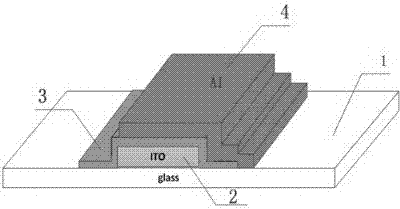
[0023] The present invention adopts the coating mode of vacuum evaporation and magnetron sputtering, has prepared the organic film photodiode that has vertical structure to be ITO / ZnPc+PbPc / Al, and aluminum cathode forms Schottky contact with the organic film on one side, and aluminum film The thickness is 20nm. The production sequence is as follows: first, use magnetron sputtering to form an ITO electrode as the anode of the diode on a clean glass substrate, then use vacuum evaporation to form a blend film of zinc phthalocyanine and lead phthalocyanine, and finally use magnetron sputtering An aluminum electrode is formed as a cathode, and the thickness of the organic film in the finished product is 120-130nm.
Embodiment 2
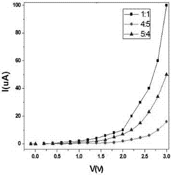
[0025] In the organic photoelectric thin film diode described in the above case, the active layer is mixed with two phthalocyanine materials, ZnPc and PbPc. By controlling the mixing ratio of the two materials, different output characteristics can be obtained to meet different needs. The barrier height of the device with the mixed mass ratio of ZnPc:PbPc of 1:1 is 0.355eV, and the influence factor n is 18.21. The barrier heights of devices with ZnPc:PbPc mixing mass ratios of 4:5 and 5:4 are 0.417eV and 0.378eV, respectively. With different mixing methods of organic materials, the Schottky barrier inside the device will also be different. The output current of the device increases with the increase of the input voltage, and the device has rectification characteristics. The maximum current of the diode formed by blending and evaporating the two materials in the active layer can reach tens of μA, which is higher than that of the diode formed by evaporating a single material.
Embodiment 3
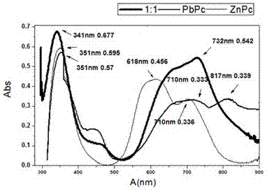
[0027] The organic photoelectric thin film diode described in the above case has a wider light-sensing wavelength band. Under the illumination of 341nm, the fill factor of the diode is FF=0.324, and the photoelectric energy conversion efficiency η=0.137%. When forward biased, the optical amplification factor of the current is in the range of 1.3-5.
PUM
| Property | Measurement | Unit |
|---|---|---|
| Thickness | aaaaa | aaaaa |
| Thickness | aaaaa | aaaaa |
| Thickness | aaaaa | aaaaa |
Abstract
Description
Claims
Application Information


