
Contacts fabric using heterostructure of metal/semiconductor nanorods and fabrication method thereof

A heterostructure, nanorod technology, applied in nanostructure fabrication, semiconductor/solid-state device fabrication, semiconductor devices, etc., can solve the problems that no one has studied to control the properties of nano-contact fabrics

Active Publication Date: 2006-07-19
LG DISPLAY CO LTD
View PDF0 Cites 3 Cited by
  • Summary
  • Abstract
  • Description
  • Claims
  • Application Information

AI Technical Summary

Problems solved by technology

However, the technology of forming artificial nanocontact fabrics on predetermined parts of nanocomponents has not yet been established, and no one has studied the technology of controlling the characteristics of nanocontact fabrics

Method used


Image

  • Contacts fabric using heterostructure of metal/semiconductor nanorods and fabrication method thereof
  • Contacts fabric using heterostructure of metal/semiconductor nanorods and fabrication method thereof
  • Contacts fabric using heterostructure of metal/semiconductor nanorods and fabrication method thereof

Examples


Embodiment approach

[0023] The contact fabric using the heterostructure of metal / semiconductor nanorods and the preparation method thereof of the present invention will be described in detail below with reference to the accompanying drawings. A detailed description of known technologies or structures would obscure and obscure the subject matter of the present invention, so details are not repeated here. The technical terms defined based on the functions of the corresponding elements used throughout the specification and claims may vary depending on a user's or operator's intention or specific circumstances. Therefore, the definitions of these technical terms should be determined based on the context of the specification and claims.

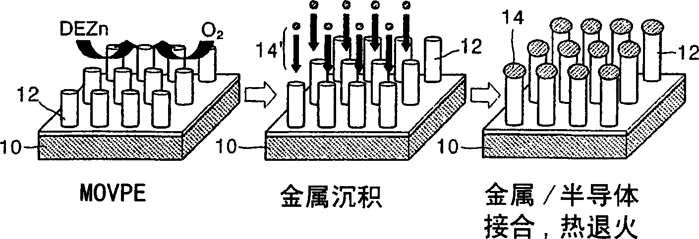
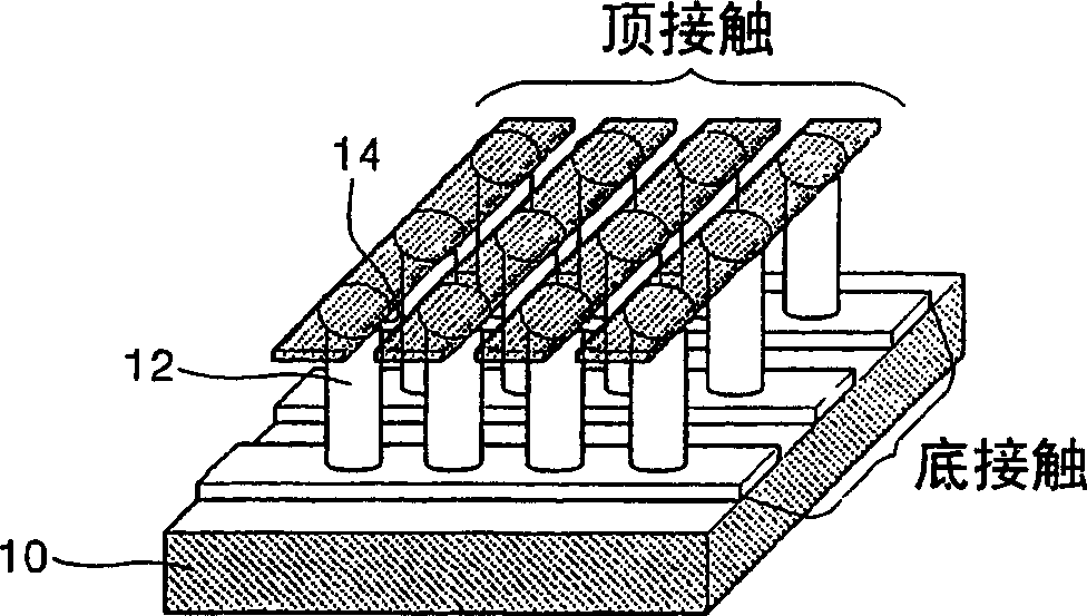
[0024] refer to figure 1 , gives an overview illustrating the inventive contact fabric using a heterostructure of metal / semiconductor nanorods and its preparation method. At this time, ZnO / semiconductor nanorods 12 are grown on the substrate 10 in a certain directi...

Embodiment 1

[0034] Growth of metal / ZnO nanorods (see figure 1 )

[0035] Gold and titanium / gold are deposited on commonly used ZnO / semiconductor nanorods aligned in a certain direction using thermal evaporation or electron beam evaporation. Here, gold was deposited to a thickness of about 20 nm, and titanium / gold was deposited to a thickness of 10 nm and 20 nm, respectively. The accelerating voltage and emission current of the electron beam used for evaporating metals are 4-20kV and 40-400mA, respectively. The pressure of the reactor is 10-5mmHg when depositing the metal, and the temperature of the substrate is room temperature. The ZnO nanorod arrays were examined using electron microscopy before and after metal deposition. It was found that the metal had been selectively deposited onto the tips of the nanorods without significant changes in the diameter and current state of the nanorods.

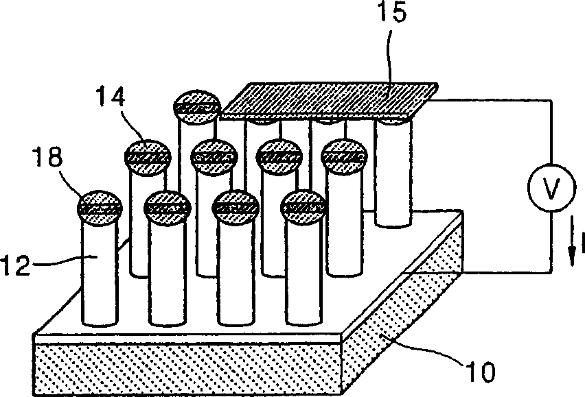
[0036] Determination of electrical properties of metal / zinc oxide nanorods (cf. Figure 4-6 )...


PUM


Abstract

Provided are a contact fabric using a heterostructure of metal / semiconductor nanorods and a method of manufacturing the same. An ohmic contact fabric having a low contact resistance or a Schottky contact fabric having a rectification characteristic is formed by selectively depositing metal of nano-sizes onto predetermined portions of zinc oxide / semiconductor nanorods and controlling the work function of the deposited metal and the interfacial characteristics of metal / zinc oxide. The contact fabric can be applied to various nano-sized electronic devices, including Schottky diodes, optical devices, and arrays thereof.

Description

technical field [0001] The present invention relates to a contact fabric using a heterostructure of metal / semiconductor nanorods and a method for preparing the same, and more particularly to a contact fabric using a heterostructure of metal / semiconductor nanorods and a method for preparing the same: wherein the contact resistance is low in ohmic Contact fabrics or Schottky contact fabrics with rectifying properties are formed by selectively depositing nanometer-sized metals onto predetermined portions of ZnO / semiconductor nanorods and controlling the work function of the deposited metal and the interfacial properties of the metal / ZnO for the use of contact fabrics in various nanoscale electronic components including Schottky diodes, optical components and arrays thereof. Background technique [0002] The amazing development of semiconductor technology since the invention of the transistor has brought about the development of large-scale integrated circuits and semiconductor ...

Claims


Application Information

Patent Timeline
Patent Type & Authority Applications(China)
IPC IPC(8): H01L33/00B82B3/00H01L21/285H01L21/44H01L29/06H01L29/22H01L29/45H01L29/47H01L31/108H01L33/20
CPCB82Y10/00H01L21/2855H01L29/22H01L29/456H01L31/108H01L29/45H01L29/452H01L33/20H01L29/47H01L21/44Y02E10/50H01L29/475H01L29/0665H01L31/035281B82Y20/00H01L21/28537H01L29/0673H01L29/0676
Inventor 李奎哲朴原一
Owner LG DISPLAY CO LTD
Learn More