Wafer-level chip structure, multi-chip stacking interconnection structure and preparation method

A wafer-level chip and chip structure technology, used in semiconductor/solid-state device manufacturing, semiconductor/solid-state device components, semiconductor devices, etc. Effect

Active Publication Date: 2020-08-18
SHANGHAI XIANFANG SEMICON CO LTD +1
View PDF3 Cites 5 Cited by
  • Summary
  • Abstract
  • Description
  • Claims
  • Application Information

AI Technical Summary

Problems solved by technology

[0003] Therefore, the present invention provides a wafer-level chip structure, a multi-chip stacked interconnection structure and a preparation method, which overcome the challenges of ultra-high selectivity ratio Si / SiOx dry etching in the prior art, difficult process or diffusion of copper atoms. Drawbacks of Active Area Contamination

Method used


Image

  • Wafer-level chip structure, multi-chip stacking interconnection structure and preparation method
  • Wafer-level chip structure, multi-chip stacking interconnection structure and preparation method
  • Wafer-level chip structure, multi-chip stacking interconnection structure and preparation method

Examples


Embodiment 1

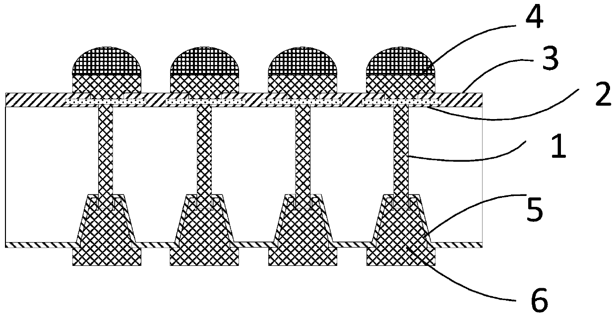
[0050] Embodiments of the present invention provide a wafer-level chip structure, such as figure 1 As shown, it includes: through-silicon via 1, and the through-silicon via is located at a preset distance from the first surface of the wafer to the second surface; the first surface of the wafer includes: an active region 2, a multi-layer Redistribution line layer 3 and bump 4; the second surface of the wafer includes: UBM layer 5 and concave insulating dielectric layer 6, the number of concave structures of the concave insulating dielectric layer 6 is the same as that of the silicon The number of through holes 1 is the same, and the bottom of the concave insulating dielectric layer is blocked by the bottom of the through-silicon hole, and the under-bump metallization layer fills the concave insulating dielectric layer and is electrically connected to the through-silicon hole. . In the embodiment of the present invention, the material filled in the TSV 1 can be copper, the bump...

Embodiment 2

[0061] An embodiment of the present invention provides a wafer-level multi-chip stacking interconnection structure, such as Figure 9 As shown, it includes: a chip bonder 8, a substrate 9 and a lead terminal 10, the chip bonder 7 is transferred to the first surface of the substrate 8, and the lead terminal 9 is formed on the second surface of the substrate, wherein,

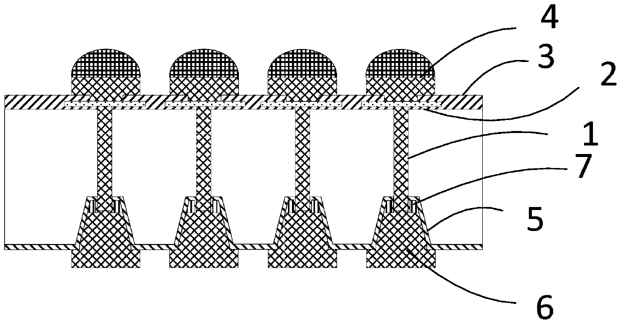
[0062] The chip bonding body 7 includes a plurality of single wafer-level chips arranged in a stack, and the multiple single wafer-level chips are directly connected through a bonding layer. The single wafer-level chips include: a first chip structure 11, And at least one second chip structure 12, the at least one second chip structure is located at the near end of the substrate, and the first chip structure is located at the far end of the substrate; the second chip structure is described in Embodiment 1 The wafer-level chip structure, such as Figure 9 It is shown that four second chip structures 12 are includ...


PUM


Abstract

The invention discloses a wafer-level chip structure, a multi-chip stacking interconnection structure and a preparation method. The wafer-level chip structure comprises a through silicon vias which are located at a preset distance from a first surface to a second surface of a wafer. The first surface of the wafer comprises an active region, a plurality of redistribution line layers and bumps; andthe second surface of the wafer comprises under-bump metallization layers and a concave insulating medium layer, wherein the number of concave structures of the concave insulating medium layer is samewith the number of the through silicon vias, the bottom of the concave insulating medium layer is separated by the bottoms of the through silicon vias, and the under-bump metallization layers fill the concave insulating medium layer and are electrically connected with the through silicon vias. The wafer-level chip structure provided by the embodiment of the invention is not sensitive to the uniformity of the depth in the TSV blind hole etching chip, and the impact on the active region from the ultrahigh selection ratio Si/SiOx dry etching and copper atom diffusion in the prior art is avoided.

Description

technical field [0001] The invention relates to the technical field of semiconductor packaging, in particular to a wafer-level chip structure, a multi-chip stacking interconnection structure and a preparation method. Background technique [0002] The key process step in the manufacture of through-silicon vias (TSVs) is the outcropping of the back of the TSV. There are two types of outcropping on the back of the TSV in the prior art: the first is to stop when the bottom of the TSV is not exposed through the thinning and polishing process, and then dry etching is used. Etch back to make TSV bumps, low-temperature SiOx / SiNx deposition, wafer polishing process, etc. realize the back exposure of TSV; the second type, firstly through the thinning and polishing process until the copper on the back of the TSV is completely exposed, and then dry etch back to make TSV bumps, low-temperature SiOx / SiNx deposition, wafer polishing, etc. to achieve TSV backside exposure. For the first so...

Claims


Application Information

Patent Timeline
Patent Type & Authority Applications(China)
IPC IPC(8): H01L23/48H01L23/485H01L21/768H01L21/60
CPCH01L23/481H01L23/4824H01L24/08H01L24/03H01L21/76898H01L24/82H01L2224/0231H01L2224/02331H01L2224/02381H01L2224/08146H01L2224/16225H01L2924/181H01L2224/73204H01L2224/32225H01L2224/11H01L2924/15311H01L2224/16145H01L2924/00012H01L2924/00
Inventor 严阳阳曹立强戴风伟
Owner SHANGHAI XIANFANG SEMICON CO LTD
Why Eureka
Try Eureka