Thin film transistor and preparation method thereof and display panel

A thin-film transistor and area technology, which is applied in transistors, semiconductor/solid-state device manufacturing, electric solid-state devices, etc., can solve the problems of adverse effects on device stability, high temperature, etc., and achieve improved self-heating effect, high pixel density, and increased heat dissipation area. Effect

Active Publication Date: 2020-08-18
BOE TECH GRP CO LTD
View PDF10 Cites 0 Cited by
  • Summary
  • Abstract
  • Description
  • Claims
  • Application Information

AI Technical Summary

Problems solved by technology

When the width-to-length ratio of the channel of the thin film transistor is large, the temperature generated by

Method used


Image

  • Thin film transistor and preparation method thereof and display panel
  • Thin film transistor and preparation method thereof and display panel
  • Thin film transistor and preparation method thereof and display panel

Examples


Embodiment Construction

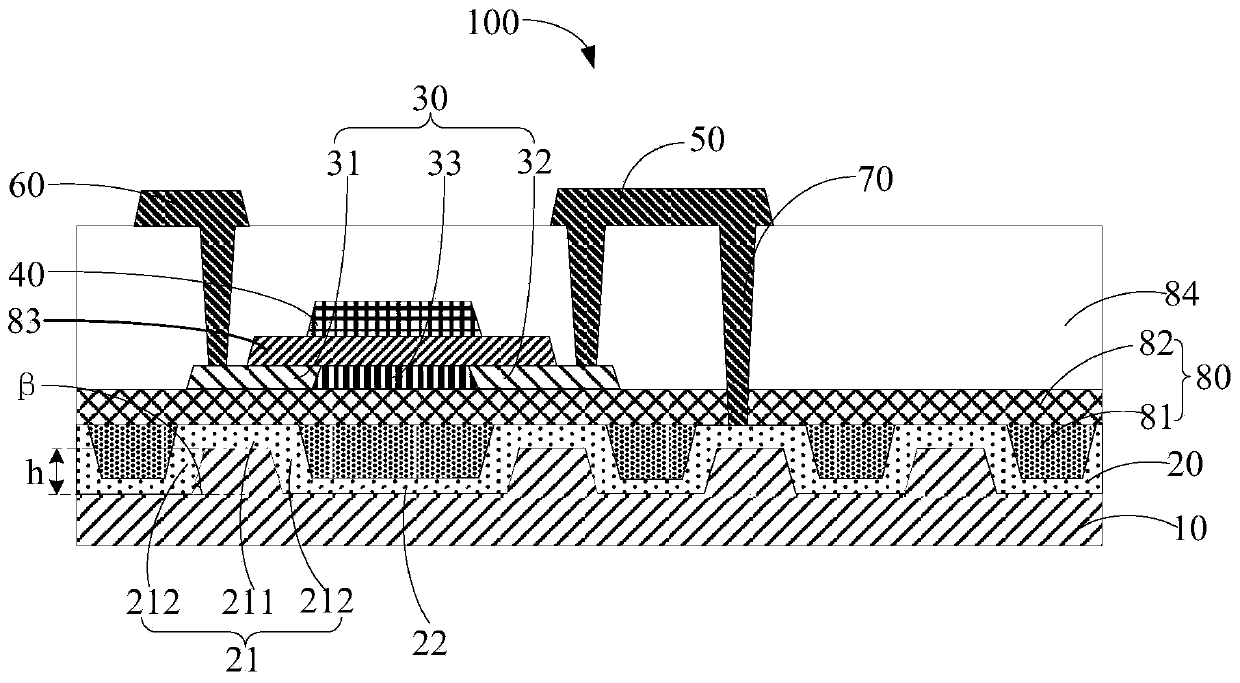
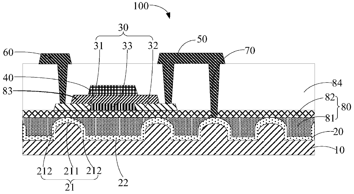
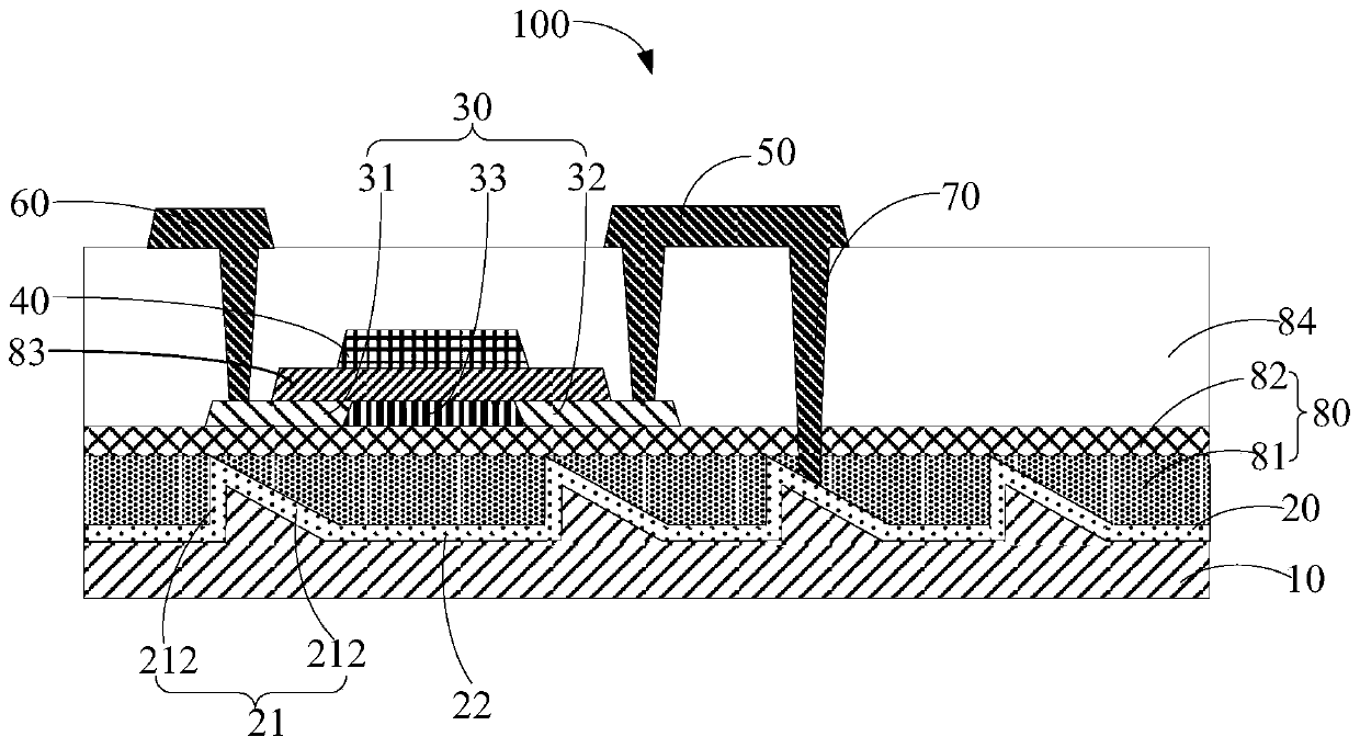
[0050] Reference will now be made in detail to the exemplary embodiments, examples of which are illustrated in the accompanying drawings. When the following description refers to the accompanying drawings, the same numerals in different drawings refer to the same or similar elements unless otherwise indicated. The implementations described in the following exemplary embodiments do not represent all implementations consistent with this application. Rather, they are merely examples of means consistent with aspects of the present application as recited in the appended claims.

[0051] The terminology used in this application is for the purpose of describing particular embodiments only, and is not intended to limit the application. Unless otherwise defined, the technical terms or scientific terms used in the application shall have the ordinary meanings understood by those skilled in the art to which the application belongs. Words such as "one" or "one" used in the specification ...


PUM

PropertyMeasurementUnit
Thicknessaaaaaaaaaa

Abstract

The invention provides a thin film transistor and a preparation method thereof and a display panel. The thin film transistor comprises a substrate, a heat dissipation layer located at one side of thesubstrate, an active layer located at one side, deviating from the substrate, of the heat dissipation layer, and a gate electrode, a first electrode and a second electrode which are located at one side, deviating from the substrate, of the active layer. The area of the surface, away from the substrate, of the heat dissipation layer is larger than the area of the orthographic projection, on the substrate, of the heat dissipation layer. The display panel comprises the thin film transistor.

Description

technical field [0001] The present application relates to the technical field of semiconductors, in particular to a thin film transistor, a manufacturing method thereof, and a display panel. Background technique [0002] In recent years, display devices based on OLED (Organic Light Emitting Diode, organic light emitting diode) have become popular display products at home and abroad because of their advantages such as self-illumination, wide viewing angle, high luminous efficiency, wide color gamut, low operating voltage, and thin panels. . [0003] The driving mode of the OLED display device is generally active driving, that is, the pixels of the display device are driven by the pixel circuit. Generally, the switch transistor in the pixel circuit adopts an oxide semiconductor transistor. When the width-to-length ratio of the channel of the thin film transistor is large, the temperature generated when the thin film transistor is in operation will be higher, which will adver...

Claims


Application Information

Patent Timeline
IPC IPC(8): H01L29/786H01L23/367H01L21/48H01L21/336
CPCH01L29/66969H01L29/7869H01L23/3672H01L21/4882
Inventor 周天民王利忠刘凤娟杨维黄睿强朝辉
Owner BOE TECH GRP CO LTD
Why Eureka
Try Eureka