Lens assembly with electric contacts, photoelectric detector and laser radar

A technology of photodetectors and electrical contacts, applied in the direction of lenses, contact parts, radio wave measurement systems, etc., can solve problems such as difficulty in reducing distance, difficulty in realizing light and thin products, space optimization settings, and inability to effectively compress device heights, etc. , to achieve the effect of optimizing the space setting, improving the efficiency of light energy utilization, and improving the ability of photoelectric signal collection

Pending Publication Date: 2020-08-25
BEIJING SURESTAR TECH
View PDF0 Cites 1 Cited by
  • Summary
  • Abstract
  • Description
  • Claims
  • Application Information

AI Technical Summary

Problems solved by technology

[0004] Because in the semiconductor process, the gold wire 2 has a height, and the gold wire 2 needs to be accommodated between the optical lenses 1, and the installation space is reserved for the gold wire 2, especially in the height direction, so the optical lens 1 The distance H between the circuit board 5 and the circuit board 5 is difficult to reduce, resulting in that the height of the device cannot be effectively compressed, and it is difficult to realize thin, light and small products and space-optimized settings

Method used


Image

  • Lens assembly with electric contacts, photoelectric detector and laser radar
  • Lens assembly with electric contacts, photoelectric detector and laser radar
  • Lens assembly with electric contacts, photoelectric detector and laser radar

Examples


Embodiment Construction

[0034] The implementation process of the technical solution of the present invention is described below in conjunction with specific embodiments, which are not intended to limit the present invention.

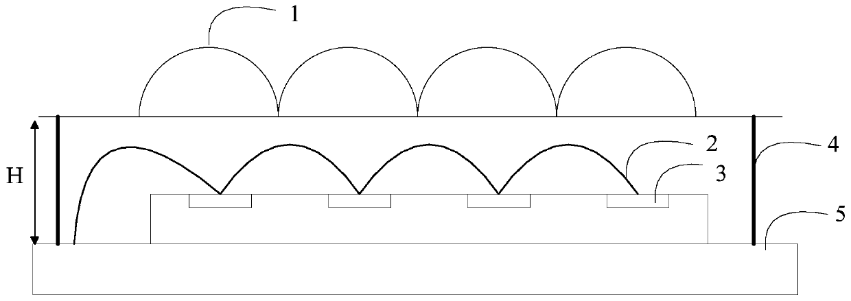
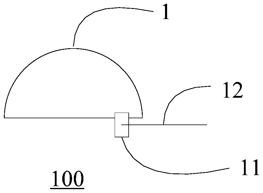
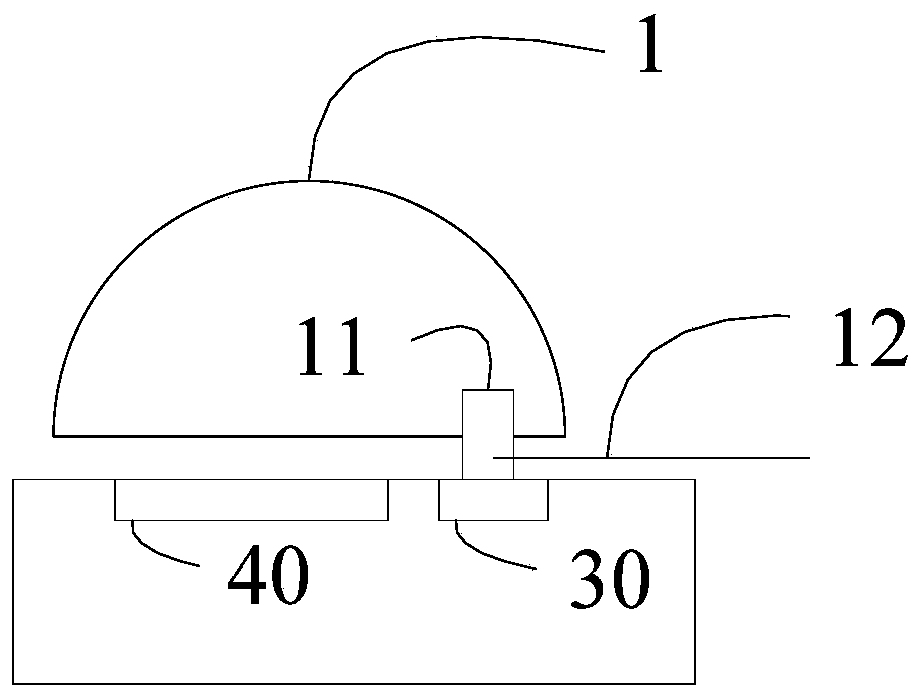
[0035] Such as Figure 2A , 2B , 2D are schematic cross-sectional structural diagrams of the lens assembly with electrical contacts of the present invention.

[0036] The lens assembly 100 includes an optical lens 1 and electrical contacts 11 .

[0037] An optoelectronic device is correspondingly disposed under the lens assembly 100 , and the electrical contact 11 is used to connect the optoelectronic device corresponding to the optical lens.

[0038] The optoelectronic device may be a photodetector. The electrical contact 11 is electrically connected to the connection part 30 of the optoelectronic device, and the connection part 30 can be a pad or an electrode. The photoactive surface 40 of the optoelectronic device faces the rear section of the optical lens 1 .

[0039] ...


PUM


Abstract

The invention discloses a lens assembly with an electric contact, a photoelectric detector and a laser radar. The lens assembly comprises an optical lens, and an electric contact which is connected with a photoelectric device corresponding to the optical lens. The packaging process of the photoelectric integrated device is simplified, the connection reliability of the integrated photoelectric device is improved, the light path design of the array type photoelectric integrated device is optimized, the photoelectric signal acquisition capability of the array type photoelectric integrated deviceis improved, the space size of the integrated device is optimized, and the light energy utilization efficiency is improved. And refined partition management is carried out on the circuit device corresponding to the lens assembly.

Description

technical field [0001] The invention relates to the field of optoelectronics, in particular to a lens assembly with electrical contacts, a photoelectric detector and a laser radar. Background technique [0002] In the prior art, some optoelectronic devices are provided with microlenses above the circuit to realize the introduction of optical signals. [0003] Such as figure 1 Shown is a schematic diagram of a circuit structure with microlenses in the prior art. The circuit board 5 is provided with a plurality of circuit device units 3 , different circuit device units 3 are connected by gold wires 2 , and the circuit device units 3 and the circuit board 5 are also connected by gold wires 2 . The optical lens 1 is erected above the plurality of circuit device units 3 through a bracket 4 . [0004] Because in the semiconductor process, the gold wire 2 has a height, and the gold wire 2 needs to be accommodated between the optical lenses 1, and the installation space is reserv...

Claims


Application Information

Patent Timeline
Patent Type & Authority Applications(China)
IPC IPC(8): G02B3/00G01S7/481H01R13/02
CPCG01S7/4816G02B3/00H01R13/02
Inventor 张珂殊
Owner BEIJING SURESTAR TECH
Why Eureka
Try Eureka