An OLED display panel and preparation method thereof, and OLED display device

A display panel and encapsulation layer technology, which is applied in semiconductor/solid-state device manufacturing, semiconductor devices, electrical components, etc., can solve the problems of low quantum efficiency of OLED display panels, improve external quantum efficiency, increase adhesion, and increase extraction rate Effect

Active Publication Date: 2022-07-12
WUHAN CHINA STAR OPTOELECTRONICS SEMICON DISPLAY TECH CO LTD
View PDF0 Cites 0 Cited by
  • Summary
  • Abstract
  • Description
  • Claims
  • Application Information

AI Technical Summary

Problems solved by technology

[0005] This disclosure provides an OLED display panel and its preparation method and OLED display device, so as to alleviate the technical problem of low external quantum efficiency of the existing OLED display panel

Method used


Image

  • An OLED display panel and preparation method thereof, and OLED display device
  • An OLED display panel and preparation method thereof, and OLED display device
  • An OLED display panel and preparation method thereof, and OLED display device

Examples


Embodiment Construction

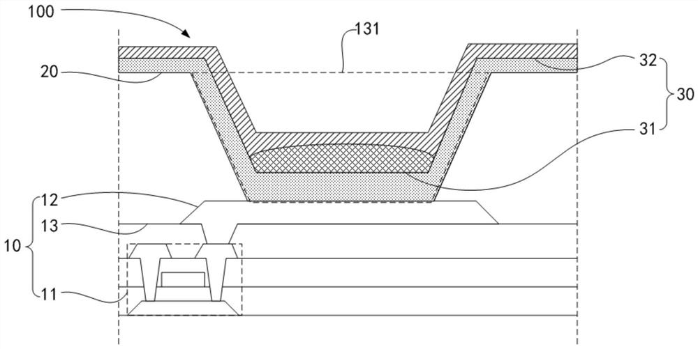
[0023] The following descriptions of the various embodiments refer to the accompanying drawings to illustrate specific embodiments in which the present disclosure may be practiced. The directional terms mentioned in this disclosure, such as [up], [down], [front], [rear], [left], [right], [inner], [outer], [side], etc., are only for reference Additional schema orientation. Accordingly, the directional terms used are used to describe and understand the present disclosure, rather than to limit the present disclosure. In the figures, structurally similar elements are denoted by the same reference numerals.

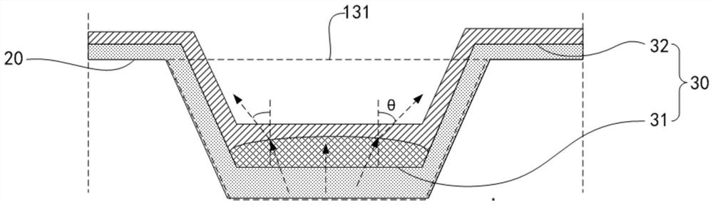
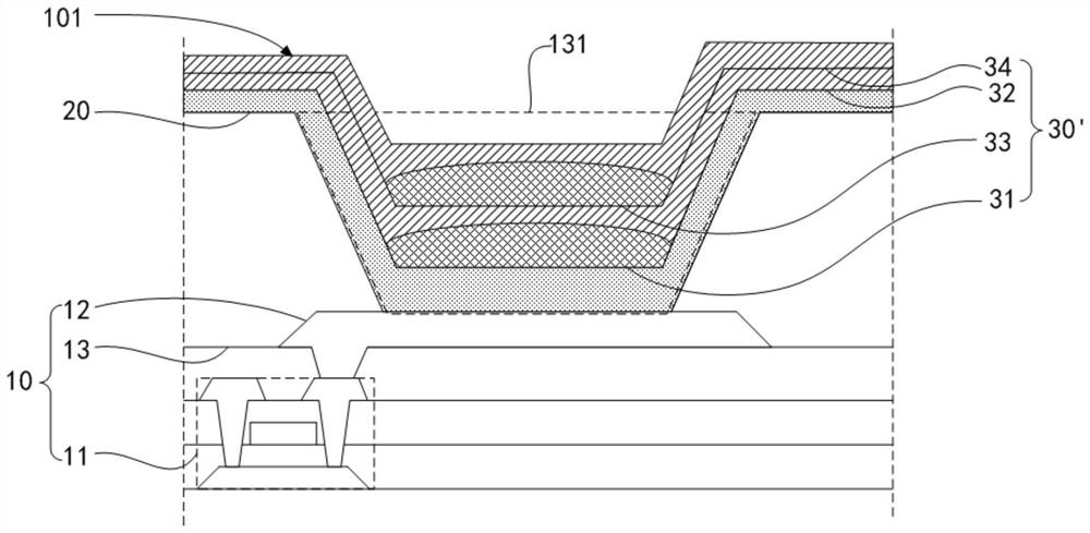
[0024] In one embodiment, as figure 1 As shown, an OLED display panel 100 is provided, which includes a driving circuit layer 10 , a light-emitting functional layer 20 and an encapsulation layer 30 . The light-emitting functional layer 20 is disposed on the driving circuit layer 10 . The encapsulation layer 30 is disposed on the light-emitting functional layer 20 and inclu...


PUM

PropertyMeasurementUnit
thicknessaaaaaaaaaa

Abstract

The present disclosure provides an OLED display panel, a manufacturing method thereof, and an OLED display device. The OLED display panel includes a driving circuit layer, a light-emitting functional layer and an encapsulation layer. The light-emitting functional layer is disposed on the driving circuit layer. The encapsulation layer is arranged on the light-emitting functional layer, and includes at least a first organic encapsulation layer and a first inorganic encapsulation layer, and the first inorganic encapsulation layer is arranged on the first organic encapsulation layer. Wherein, the contact surface of the first organic encapsulation layer and the first inorganic encapsulation layer has a convex arc structure. In order to improve the extraction rate of light, thereby improving the external quantum efficiency.

Description

technical field [0001] The present disclosure relates to the field of display technology, and in particular, to an OLED display panel, a method for manufacturing the same, and an OLED display device. Background technique [0002] Organic Light Emitting Diode (OLED) display products have the advantages of thinness, fast response, wide viewing angle, high contrast, and flexibility. Therefore, OLED is considered to be a new generation of flat panel display products and technologies after Liquid Crystal Display (LCD), and has received more and more attention and applications. [0003] The OLED display panel includes a base layer, a thin film transistor (Thin Film Transistor, TFT) driving layer, an OLED light-emitting layer, an encapsulation layer (Thin Film Encapsulation, TFE) and the like from bottom to top. The light-emitting principle of the OLED display panel is to deposit an OLED light-emitting layer between two electrodes, and pass a current to the OLED light-emitting lay...

Claims


Application Information

Patent Timeline
Patent Type & Authority Patents(China)
IPC IPC(8): H01L51/52H01L27/32
CPCH10K59/00H10K50/84H10K50/85H10K50/844
Inventor 李朝
Owner WUHAN CHINA STAR OPTOELECTRONICS SEMICON DISPLAY TECH CO LTD
Why Eureka
Try Eureka