Display substrate, preparation method thereof and display device

A technology for display substrates and substrates, used in semiconductor/solid-state device manufacturing, electrical components, electrical solid-state devices, etc., can solve the problems of large thickness of polarizers on display substrates, save process targets, reduce process complexity, reduce Effects of preparation steps

Pending Publication Date: 2020-08-25
BOE TECH GRP CO LTD
View PDF4 Cites 0 Cited by
  • Summary
  • Abstract
  • Description
  • Claims
  • Application Information

AI Technical Summary

Problems solved by technology

[0004] The technical problem to be solved by the embodiments of the present invention is to provide a display substrate and its preparatio...

Method used


Image

  • Display substrate, preparation method thereof and display device
  • Display substrate, preparation method thereof and display device
  • Display substrate, preparation method thereof and display device

Examples


Embodiment Construction

[0045] The specific implementation manners of the present invention will be further described in detail below in conjunction with the accompanying drawings and examples. The following examples are used to illustrate the present invention, but are not intended to limit the scope of the present invention. It should be noted that, in the case of no conflict, the embodiments in the present application and the features in the embodiments can be combined arbitrarily with each other.

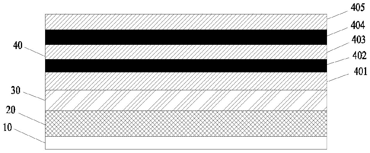
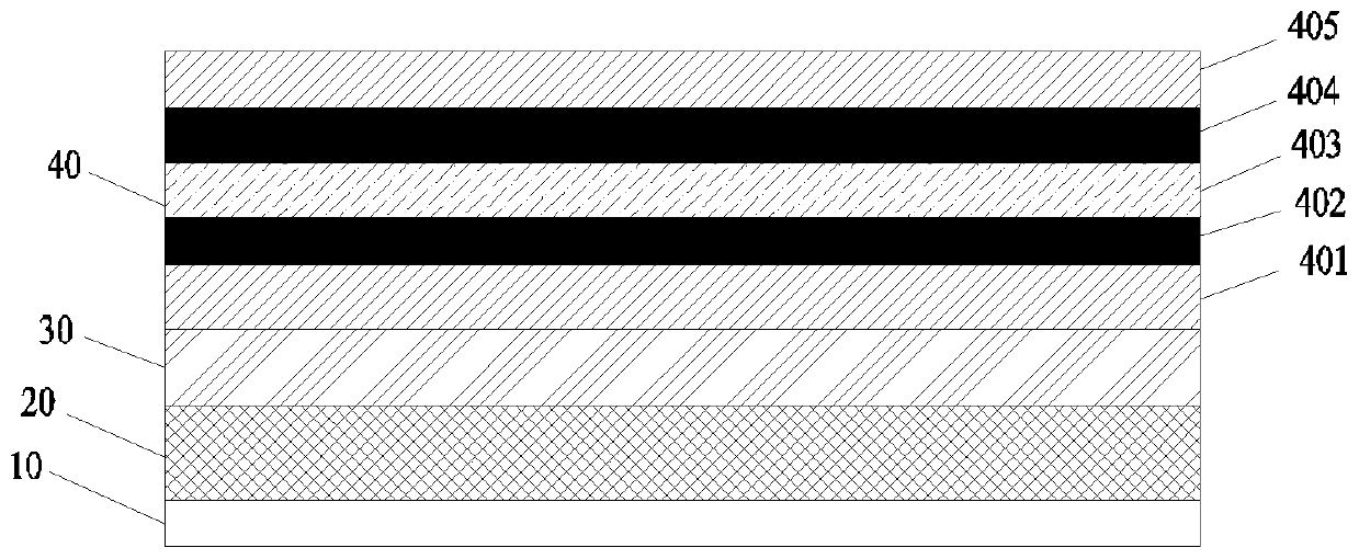
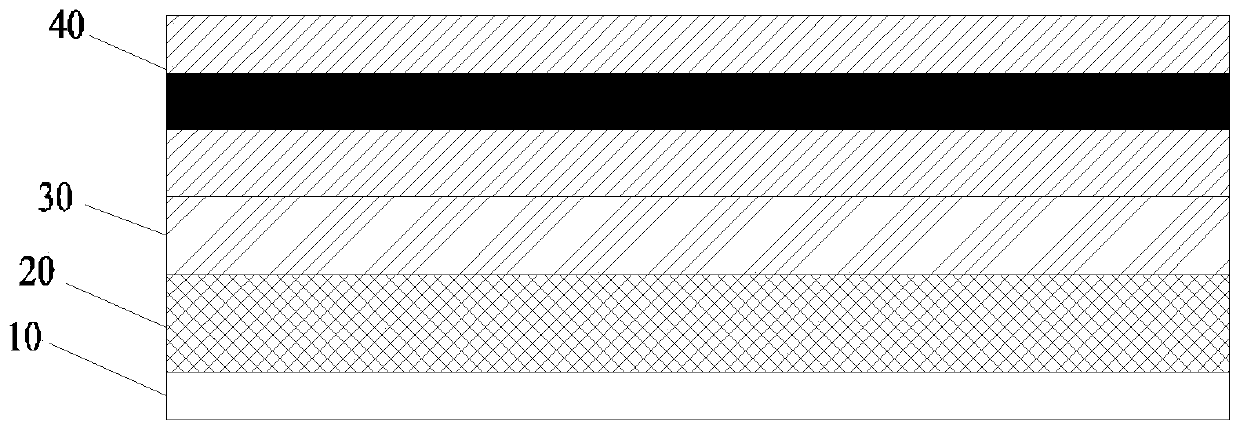
[0046] An embodiment of the present invention provides a display substrate. The embodiment of the present invention shows that the main structure of the substrate includes a base, a light-emitting unit disposed on the base, and an anti-reflection film layer disposed on the light-emitting unit, and the anti-reflection film layer includes a light-emitting unit disposed on the light-emitting unit. a first dielectric layer, a first metal layer disposed on the first dielectric layer, a second dielectric la...


PUM


Abstract

The invention provides a display substrate, a preparation method thereof and a display device. The display substrate comprises a substrate body, a light-emitting unit arranged on the substrate body and an antireflection film layer arranged on the light-emitting unit. The antireflection film layer comprises a first dielectric layer arranged on the light-emitting unit, a first metal layer arranged on the first dielectric layer, a second dielectric layer arranged on the first metal layer, a second metal layer arranged on the second dielectric layer and a third dielectric layer arranged on the second metal layer; and the problem that the thickness of the display substrate is large due to a polaroid is solved.

Description

technical field [0001] The invention relates to the field of display technology, in particular to a display substrate, a preparation method thereof, and a display device. Background technique [0002] Organic Light Emitting Diode (OLED) is an active light-emitting display device, which has the advantages of self-illumination, wide viewing angle, high contrast, low power consumption, wide color gamut, light and thin, and can be shaped. With the continuous development of display technology, OLED technology is increasingly used in flexible displays and transparent displays. Transparent display is an important branch of display technology. It refers to image display in a transparent state. The viewer can not only see the image in the display device, but also see the scene behind the display device, which can realize virtual reality / augmented reality ( Virtual Reality / Augmented Reality, VR / AR) and 3D display functions. [0003] When an OLED display is viewed in an external envi...

Claims


Application Information

Patent Timeline
IPC IPC(8): H01L51/52H01L51/56H01L27/32
CPCH10K59/40H10K50/865H10K71/00
Inventor 王纯阳王和金李良坚刘浩
Owner BOE TECH GRP CO LTD
Why Eureka
Try Eureka