
Milling device for carrying out cutting on PCB

A milling device, PCB board technology, applied in the direction of positioning device, milling machine equipment, milling machine equipment details, etc., can solve the problems of inability to adjust the position of the milling cutter, can only cut off, and low efficiency of board splitting, so as to improve milling efficiency and reduce Effect of low productivity and reduced milling time

Pending Publication Date: 2020-08-28
赛尔康(贵港)有限公司
View PDF0 Cites 1 Cited by
  • Summary
  • Abstract
  • Description
  • Claims
  • Application Information

AI Technical Summary

Problems solved by technology

[0006] 2. The PCB size is large, but it needs to be designed into an irregular shape for subsequent assembly, and the excess part can only be cut off
[0007] The splitting device in the prior art is a single-head splitting device, and there are many moving points on a single head, and six points in a row need to be moved six times, and the position of the milling cutter cannot be adjusted, so the splitting efficiency is low

Method used


Image

  • Milling device for carrying out cutting on PCB
  • Milling device for carrying out cutting on PCB
  • Milling device for carrying out cutting on PCB

Examples


Embodiment Construction

[0034] The present invention will be described in further detail below in conjunction with the accompanying drawings.

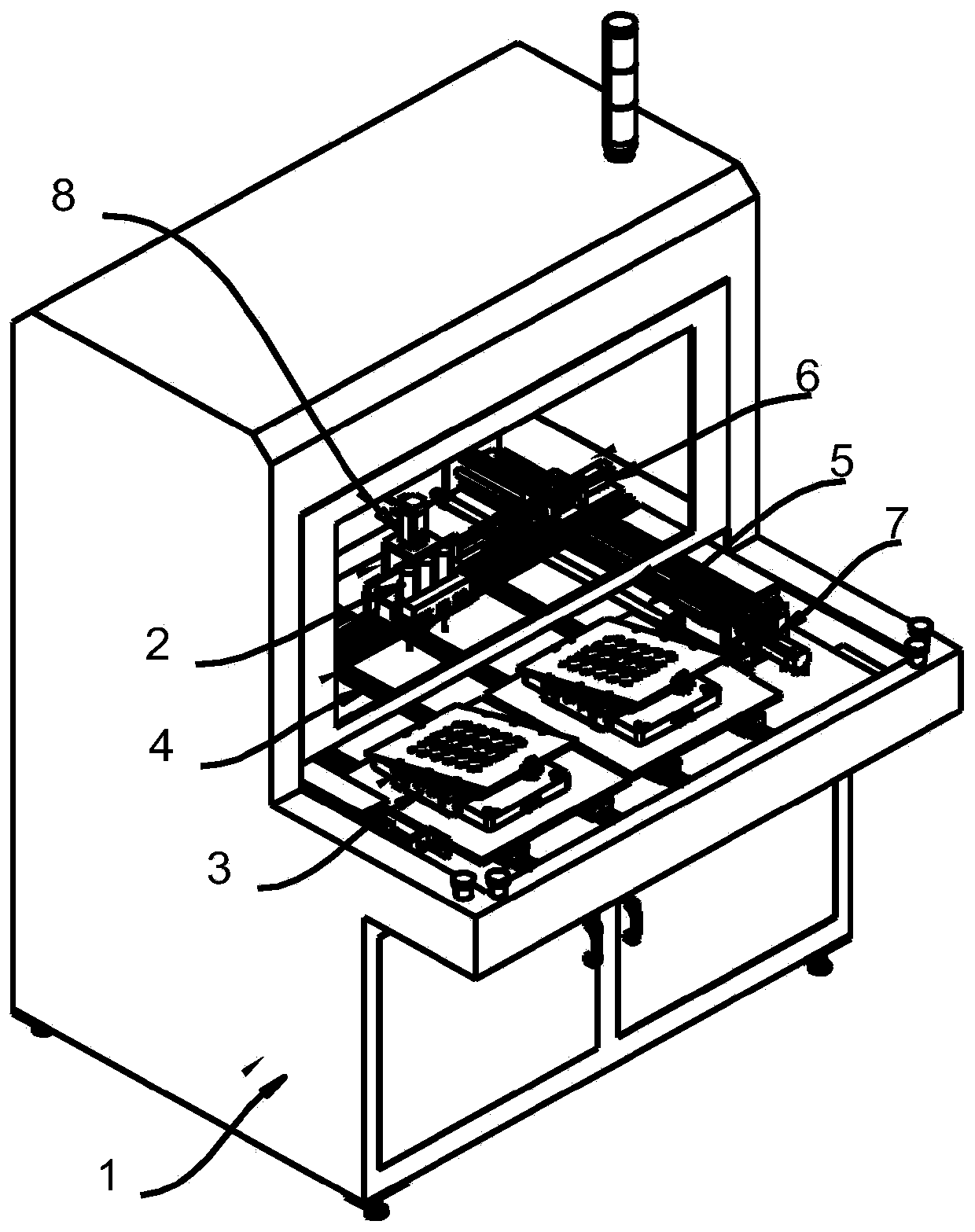
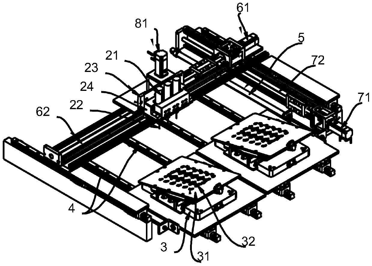
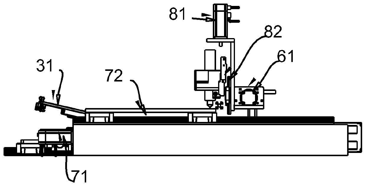
[0035] Figure 1 to Figure 5 A milling device for dividing a PCB board according to an embodiment of the present invention is schematically shown. As shown in the figure, the device includes a frame 1, a moving mechanism and a milling mechanism 2. Both the moving mechanism and the milling mechanism 2 are arranged on the frame 1, and the milling mechanism 2 is connected with the moving mechanism. The moving mechanism can drive the milling mechanism 2 to move , The milling mechanism 2 includes a plurality of splitting spindles 21 . The frame 1 is provided with a control cabinet for setting and controlling the operation of the entire device.

[0036] The present invention is provided with a plurality of board-dividing main shafts 21, and these board-dividing main shafts 21 can move flexibly by moving mechanism, and the cutting tool 22 that is used for milling ...


PUM


Abstract

The invention discloses a milling device for carrying out cutting on a PCB (Printed Circuit Board). The milling device for carrying out cutting on the PCB (Printed Circuit Board) comprises a rack, a moving mechanism and a milling mechanism, the moving mechanism and the milling mechanism are both arranged on the rack, the milling mechanism is connected with the moving mechanism, the milling mechanism can be driven by the moving mechanism to carry out movement, and the milling mechanism comprises a plurality of board splitting main shafts. The milling device for carrying out cutting on the PCB (Printed Circuit Board) is provided with the plurality of board splitting main shafts, the board splitting main shafts can carry out flexible movement through the moving mechanism, and cutters used formilling are mounted on the board splitting main shafts, so that the milling time (CT) of the PCB is further shortened, the machining efficiency is improved, the low productivity caused by overlong CTis reduced, and the productivity (UPH) of a production line is improved to meet the requirements of customers.

Description

technical field [0001] The invention relates to the field of on-line subdivision of PCB boards in the electronic and electrical industry, in particular to a milling device for subdividing PCB boards. Background technique [0002] The printed circuit board is often referred to as the PCB, and the components on the PCB are called the circuit board assembly or PCBA. The components on the board can be SMT components, plug-in components, or assemblies. [0003] In the PCB production process, in order to assist SMT patches, plug-ins, etc., the board edges added on both sides or four sides of the PCB board are not part of the PCB board and will be cut off after the PCB production is completed. The process of cutting off the edge of the board is called splitting. In the process of SMT placement, reflow soldering, AOI testing and other processes, the PCB board is automatically run on the track, and the increase of the board edge can prevent the track from touching the components on ...

Claims


Application Information

Patent Timeline
Patent Type & Authority Applications(China)
IPC IPC(8): B23C3/00B23Q1/25B23Q3/06
CPCB23C3/00B23Q1/25B23Q3/062
Inventor 李博睿伍睿康陆小竞
Owner 赛尔康(贵港)有限公司
Learn More