Non-contact heating flip-chip bonding process method

A non-contact, process-based technology, applied in the field of non-contact heating flip-chip soldering, can solve the problems of difficult cleaning of flux and weak welding, so as to achieve no risk of displacement, avoid rapid increase of oxides, simplify The effect of the process

Active Publication Date: 2020-09-11
NO 24 RES INST OF CETC
View PDF8 Cites 2 Cited by
  • Summary
  • Abstract
  • Description
  • Claims
  • Application Information

AI Technical Summary

Problems solved by technology

[0004] The technical problem to be solved by the present invention is to provide a non-contact heating flip-chip welding process to solve the problems that the flux is not easy to clean and the soldering is not firm in the traditional process.

Method used


Image

  • Non-contact heating flip-chip bonding process method
  • Non-contact heating flip-chip bonding process method
  • Non-contact heating flip-chip bonding process method

Examples


Embodiment Construction

[0028] The present invention will be further described below in conjunction with accompanying drawing.

[0029] In the description of the present invention, unless otherwise specified and limited, it should be noted that the term "connection" should be understood in a broad sense, for example, it can be a mechanical connection or an electrical connection, or it can be the internal communication of two elements, it can be Directly connected or indirectly connected through an intermediary, those skilled in the art can understand the specific meanings of the above terms according to specific situations.

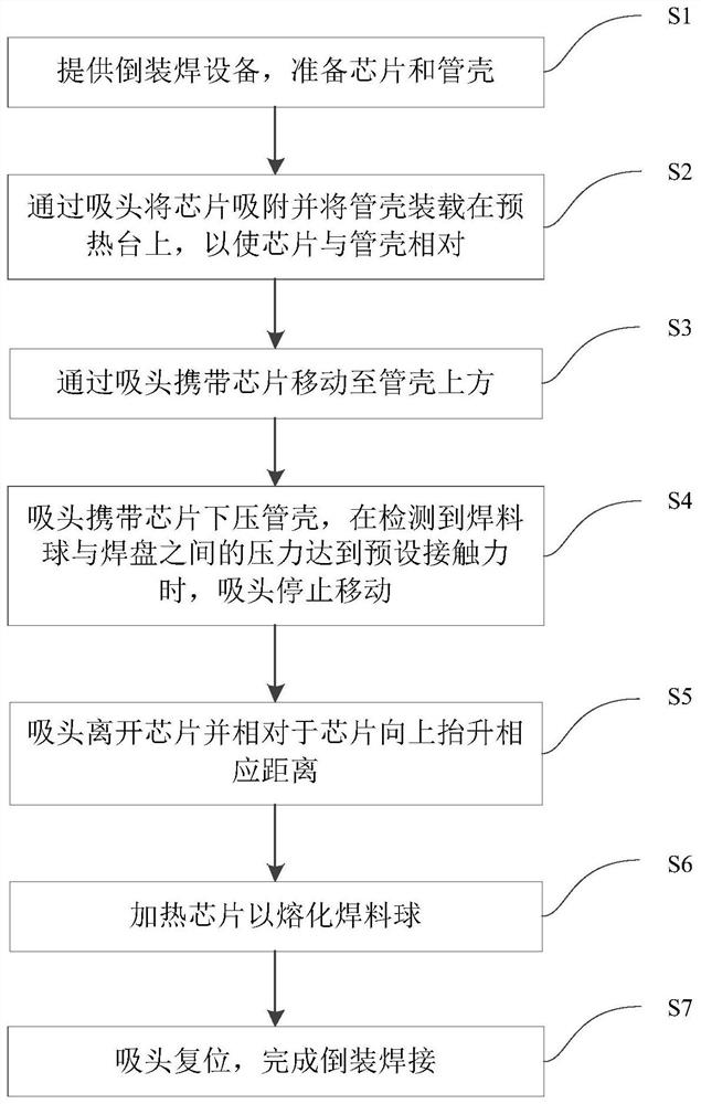
[0030] Such as figure 1 Shown is a flow chart of a preferred embodiment of the non-contact heating flip-chip process method of the present invention. The flip-chip welding process method of non-contact heating of the present invention specifically comprises the following steps:

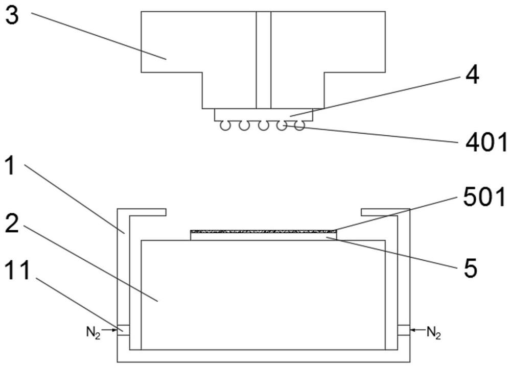
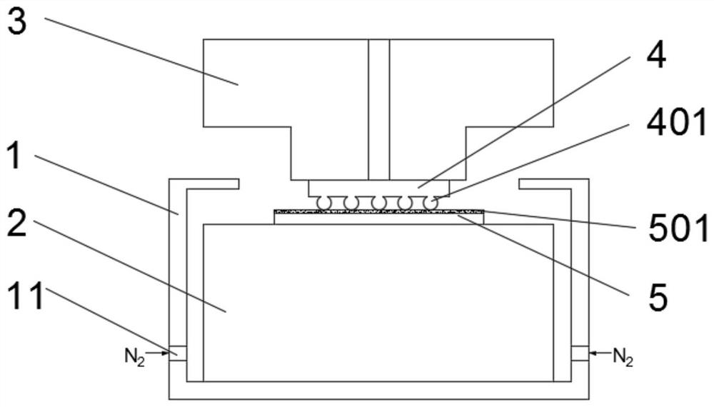
[0031] S1: Provide a flip-chip welding device with a protection device 1, a preheating table 2 and...


PUM


Abstract

The invention discloses a non-contact heating flip-chip bonding process method, which comprises the following steps: providing flip-chip bonding equipment, and preparing a chip with solder ball bumpsand a tube shell with a bonding pad; enabling the face, provided with the solder ball bumps, of the chip to be opposite to the tube shell; moving a suction head carrying the chip to a corresponding welding position above the tube shell; pressing the tube shell downwards by the suction head carrying the chip, and stopping movement of the suction head when the pressure between the solder ball bumpand the bonding pad reaches the preset contact force; leaving the chip by the suction head and lifting the chip upwards; starting suction head heating, heating the surface of the suction head to a preset temperature, maintaining the temperature for corresponding time, and heating the chip to melt the solder ball; and stopping heating of the suction head and lifting the suction head to reset, and completing welding of the chip and the tube shell. According to the process method, the whole process flow is simplified, the production efficiency is greatly improved, the chip and the tube shell havea self-alignment effect in the welding process, and a problem that the solder ball bumps are compressed unevenly due to mechanical stress between the solder ball bumps and the bonding pads can be effectively solved.

Description

technical field [0001] The invention relates to an integrated circuit packaging process, in particular to a non-contact heating flip-chip welding process method. Background technique [0002] The flip-chip welding process (flip-chip) has a wide range of applications in high-density, high-reliability integrated circuit packaging processes. The mainstream process method is: substrate or shell printing flux → chip flip-chip welding (using flux to adhere the chip to the surface of the shell or substrate) → reflow → cleaning the residual flux between the gap between the chip and the substrate. [0003] There are many problems with the traditional process method: the flux remaining between the chip and the substrate is not easy to clean, especially for oil-soluble flux; if no flux is used, the chip and the substrate are pre-attached Reflow after bonding, because there is no adhesive force of flux between the chip and the substrate, relative displacement easily occurs, which event...

Claims


Application Information

Patent Timeline
Patent Type & Authority Applications(China)
IPC IPC(8): H01L21/56H01L23/488
CPCH01L21/563H01L23/488H01L2224/75H01L2224/81191
Inventor 李金龙熊化兵李双江张文烽王旭光江凯
Owner NO 24 RES INST OF CETC
Why Eureka
Try Eureka