Stacking structure and method for chips with central bonding points

A stacking structure and bonding point technology, which is applied in the direction of electrical components, transistors, and electric solid-state devices, can solve the problems that silicon wafers cannot be stacked high and stacked, and achieve the effect of rich chip selection and reduced module volume

Inactive Publication Date: 2020-09-15
XIAN MICROELECTRONICS TECH INST
View PDF4 Cites 2 Cited by
  • Summary
  • Abstract
  • Description
  • Claims
  • Application Information

AI Technical Summary

Problems solved by technology

[0008] The object of the present invention is to overcome the above-mentioned shortcoming of prior art, provide a kind of stacking structure and method of center bonding point chip, be used for solving the chip of existing high-density bonding point of center bonding point, because bonding point is in the center, cannot Technical problems of using traditional silicon chip stacking method

Method used


Image

  • Stacking structure and method for chips with central bonding points
  • Stacking structure and method for chips with central bonding points
  • Stacking structure and method for chips with central bonding points

Examples


Embodiment Construction

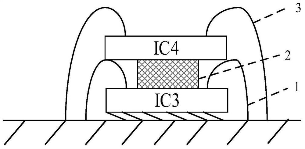
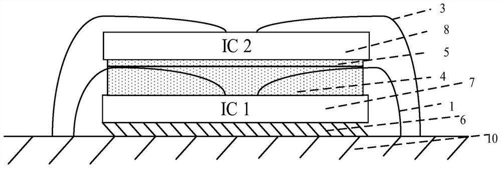
[0037] The present invention is described in further detail below in conjunction with accompanying drawing:

[0038] In the description of the present invention, it should be noted that the terms "center", "upper", "lower", "left", "right", "vertical", "horizontal", "inner", "outer" etc. The indicated orientation or positional relationship is based on the orientation or positional relationship shown in the drawings, and is only for the convenience of describing the present invention and simplifying the description, rather than indicating or implying that the referred device or element must have a specific orientation, or in a specific orientation. construction and operation, and therefore cannot be construed as limiting the present invention; the terms "first", "second", and "third" are used for descriptive purposes only, and cannot be construed as indicating or implying relative importance; in addition, unless otherwise Clearly stipulated and limited, the terms "installation"...


PUM


Abstract

The invention discloses a stacking structure and method for chips with central bonding points, and the structure effectively solves the lowest assembly problem of the chips with the central bonding points in an insulating glue stacking mode, enables the assembly density of a module to be greater than or equal to 200%, and reduces the size of the module. Due to the fact that the stacking mode can be compatible with processes such as bare chip welding, chip bonding, pressure welding and packaging, the method can solve the problem of stacking of chips with center bonding points, the chips can beeffectively integrated in a high-density mode, model selection of the chips with module function integration of the same function is richer, and the method is an effective integration method for system integration.

Description

【Technical field】 [0001] The invention belongs to the field of integrated circuits, and in particular relates to a stacking structure and method of central bond point chips. 【Background technique】 [0002] With the continuous innovation and development of technology, fields such as aviation and aerospace vehicles and weapons continue to require faster, smaller and lighter computer main parts. Therefore, in recent years, driven by this rigid demand, system integration technology has developed vigorously, and various assembly and packaging technologies have emerged continuously. Make the computer system develop towards miniaturization and light weight. As a key assembly technology, chip stack assembly reduces the assembly density of system integration technology and effectively promotes the development of micro system integration products. [0003] see figure 1 , the existing stacked chip assembly technology is to avoid the bonding point at the edge of the chip after the fi...

Claims


Application Information

Patent Timeline
Patent Type & Authority Applications(China)
IPC IPC(8): H01L25/065H01L21/98H01L27/108
CPCH01L25/0657H01L25/50H01L2225/0651H01L2225/06572H10B12/00
Inventor 李晗张欲欣冯春苗张现顺郭清军
Owner XIAN MICROELECTRONICS TECH INST
Why Eureka
Try Eureka