Array substrate and touch display panel

A technology of array substrates and touch electrodes, applied in instruments, semiconductor devices, computing, etc., can solve the problems of touch stripes on touch display panels and affect testing, so that the sensing area is not affected and the problem of stripes is avoided Effect

Pending Publication Date: 2020-09-18
KUSN INFOVISION OPTOELECTRONICS
View PDF9 Cites 0 Cited by
  • Summary
  • Abstract
  • Description
  • Claims
  • Application Information

AI Technical Summary

Problems solved by technology

For the in-cell touch display panel, since the touch electrode is formed by dividing the common electrode into multiple pieces, during the test, the parasitic capacitance between the scan line of the array substrate and the touch electrode will make the touch display panel appear Touch stripes, affect the test

Method used


Image

  • Array substrate and touch display panel
  • Array substrate and touch display panel
  • Array substrate and touch display panel

Examples


no. 1 example

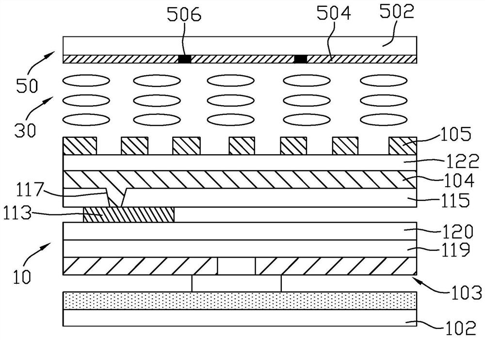
[0024] figure 1 It is a schematic cross-sectional structure diagram of a touch display panel according to an embodiment of the present invention. Please refer to figure 1 The touch display panel provided in this embodiment includes an array substrate 10 , a liquid crystal layer 30 and an opposite substrate 50 , and the liquid crystal layer 30 is located between the array substrate 10 and the opposite substrate 50 . The array substrate 10 includes a first substrate 102, a switching element 103, a common electrode 104 and a pixel electrode 105, the switching element 103, the common electrode 104 and the pixel electrode 105 are stacked on the first substrate 102, and the common electrode 104 and the pixel electrode 105 are stacked on the first substrate 102. 105 insulation interval settings. Please refer to figure 2 , the common electrode 104 is divided into a plurality of touch electrodes 107 to realize the touch function. Please refer to image 3 , a plurality of pixel uni...

no. 2 example

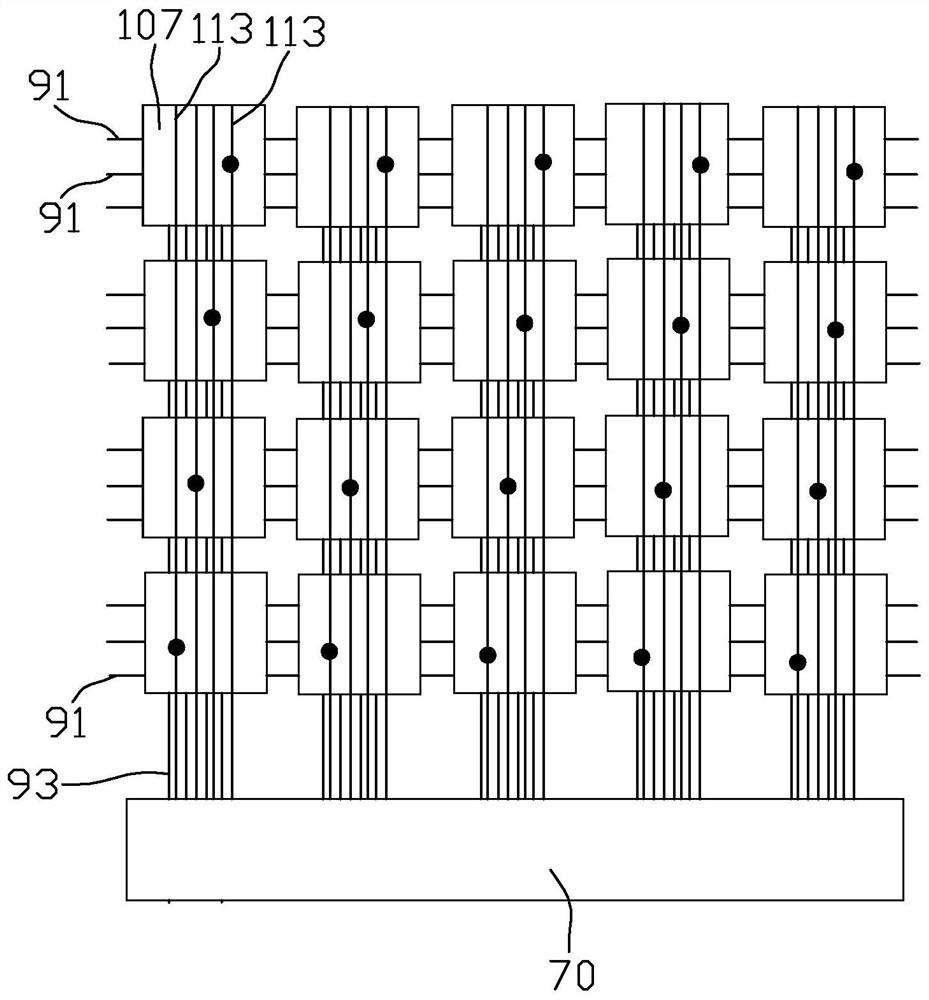
[0037] Please refer to Figure 4, the structure of the touch display panel of this embodiment is basically the same as that of the touch display panel of the first embodiment, the difference is that in this embodiment, the sub-electrodes 111 of the same touch electrode 107 are connected to the The adjacent sub-electrodes 111 are electrically connected, and one touch electrode 107 only needs to pass through one via hole 117 to be electrically connected to the touch signal line 113 , without each sub-electrode 111 passing through one via hole 117 and the touch signal line respectively. 113 is electrically connected, which can greatly reduce the number of openings 117 and simplify the manufacturing process.

[0038] Specifically, the connection portion 124 is provided corresponding to the position of the data line 93 , that is, corresponding to the position of the light shielding layer 506 of the opposite substrate 50 .

[0039] Specifically, the connecting portion 124 may be di...

no. 3 example

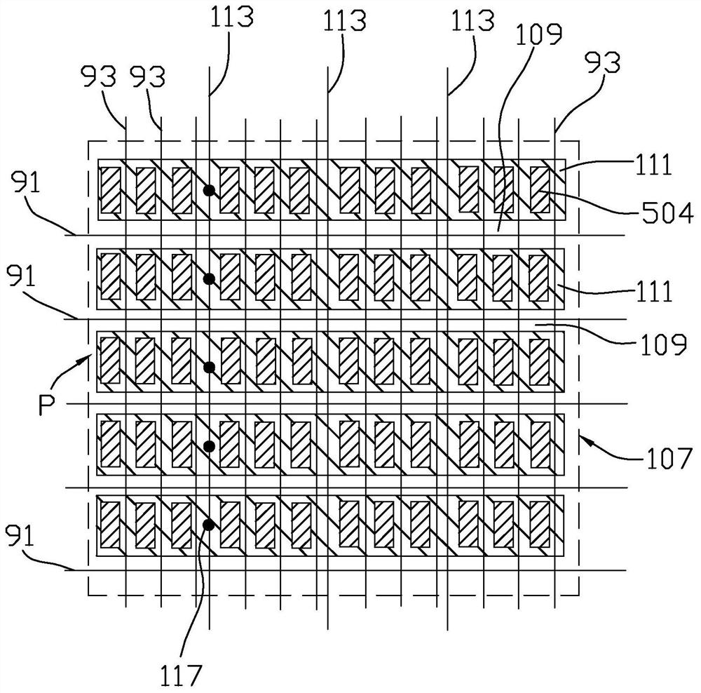
[0041] Please refer to Figure 5 The structure of the touch display panel of this embodiment is basically the same as that of the touch display panel of the first embodiment. The difference is that in this embodiment, two scan lines 91 are arranged every two rows of pixel units P, which are located above The scanning line 91 of the upper part is connected to the switching element 103 in the upper pixel unit P, and the lower scanning line 91 is connected to the switching element 103 in the lower pixel unit P. Each sub-electrode 111 is provided corresponding to the pixel units P in two rows. In this way, the number of hollows 109 on each touch electrode 107 can be reduced, which simplifies the manufacturing process and increases the sensing area of ​​the touch electrode 107 .


PUM


Abstract

The invention provides an array substrate and a touch display panel. The array substrate comprises a first substrate, a switch element, a common electrode and a pixel electrode, wherein the switch element, the common electrode and the pixel electrode are stacked on the first substrate; the common electrode and the pixel electrode are arranged at an interval in an insulating mode; the common electrodes are divided into a plurality of touch electrodes, the array substrate is further limited by transverse scanning lines and longitudinal data lines to form a plurality of pixel units, and hollowed-out parts are formed in the positions, corresponding to the scanning lines, of the touch electrodes. The invention discloses an array substrate and a touch display panel. Due to the fact that the positions, corresponding to the scanning lines, of the touch electrodes are hollowed out, parasitic capacitance between the common electrodes serving as the touch electrodes and the scanning lines is verysmall, coupling of energization of the scanning lines to the common electrodes is very small, the cross grain problem in the testing process is avoided, and the induction area of the touch electrodesis basically not affected.

Description

technical field [0001] The present invention relates to the field of touch technology, and in particular, to an array substrate and a touch display panel. Background technique [0002] The liquid crystal display panel has the advantages of good picture quality, small size, light weight, low driving voltage, low power consumption, no radiation and relatively low manufacturing cost, and is dominant in the field of flat panel display. With the continuous advancement of display technology, touch devices have gradually spread throughout people's lives. At present, an indium tin oxide (Indium Tin Oxides, ITO) transparent conductive film is generally used as a touch electrode of a touch device. Due to the mature development of liquid crystal display panel technology in recent years, it has gradually become a trend to combine touch technology with liquid crystal display panels. [0003] At present, the touch panel can be classified into an external touch display panel, an overlay ...

Claims


Application Information

Patent Timeline
IPC IPC(8): G02F1/1362G02F1/1343G02F1/1333G06F3/041H01L27/12
CPCG02F1/136286G02F1/136227G02F1/134309G02F1/13338G06F3/0412H01L27/124
Inventor 李海波
Owner KUSN INFOVISION OPTOELECTRONICS
Why Eureka
Try Eureka