Manufacturing method of cavity-type film bulk acoustic resonator (FBAR)

A thin-film bulk acoustic wave and resonator technology, applied in electrical components, impedance networks, etc., can solve the problems of stress concentration transducer damage and long release time, and achieve the effect of small parasitic capacitance, suitable for mass production, and simple process

Inactive Publication Date: 2011-02-16
CHINA ELECTRONICS TECH GRP NO 26 RES INST
View PDF4 Cites 26 Cited by
  • Summary
  • Abstract
  • Description
  • Claims
  • Application Information

AI Technical Summary

Problems solved by technology

[0006] In order to overcome the sacrificial layer CMP polishing, long release time of the sacrificial layer, stress concentration phenomenon caused by uneven steps of the sacrificial layer, and damage to the transducer caused by the release time of the sacrificial layer etc., the present invention provides a new manufacturing method of thin film bulk acoustic resonator. The thin film bulk acoustic resonator produced by the present invention has no sacrificial layer, and does not need the chemic

Method used


Image

  • Manufacturing method of cavity-type film bulk acoustic resonator (FBAR)
  • Manufacturing method of cavity-type film bulk acoustic resonator (FBAR)
  • Manufacturing method of cavity-type film bulk acoustic resonator (FBAR)

Examples


Embodiment Construction

[0013] The performance of the present invention will be further described in detail below in conjunction with the accompanying drawings, the working principle of the present invention and experiments.

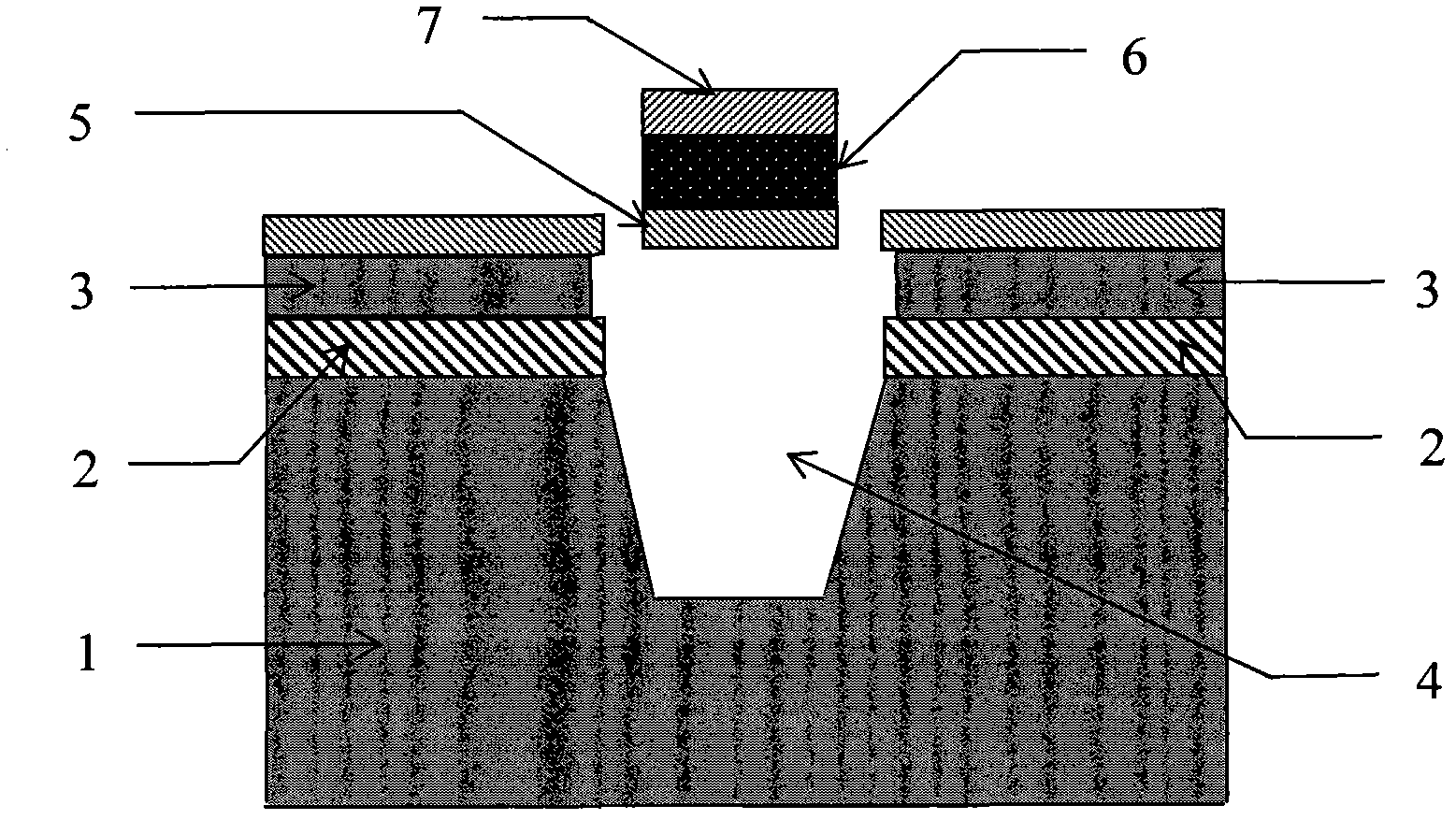
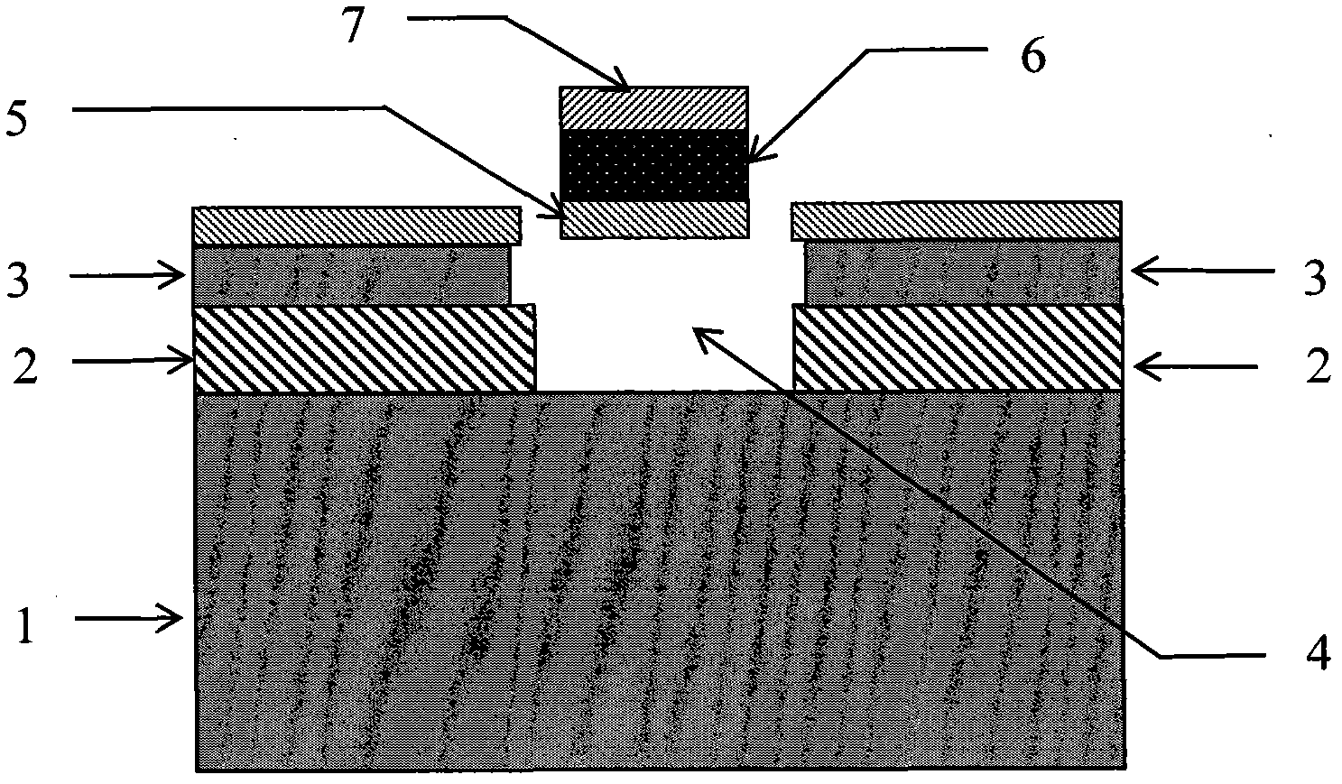
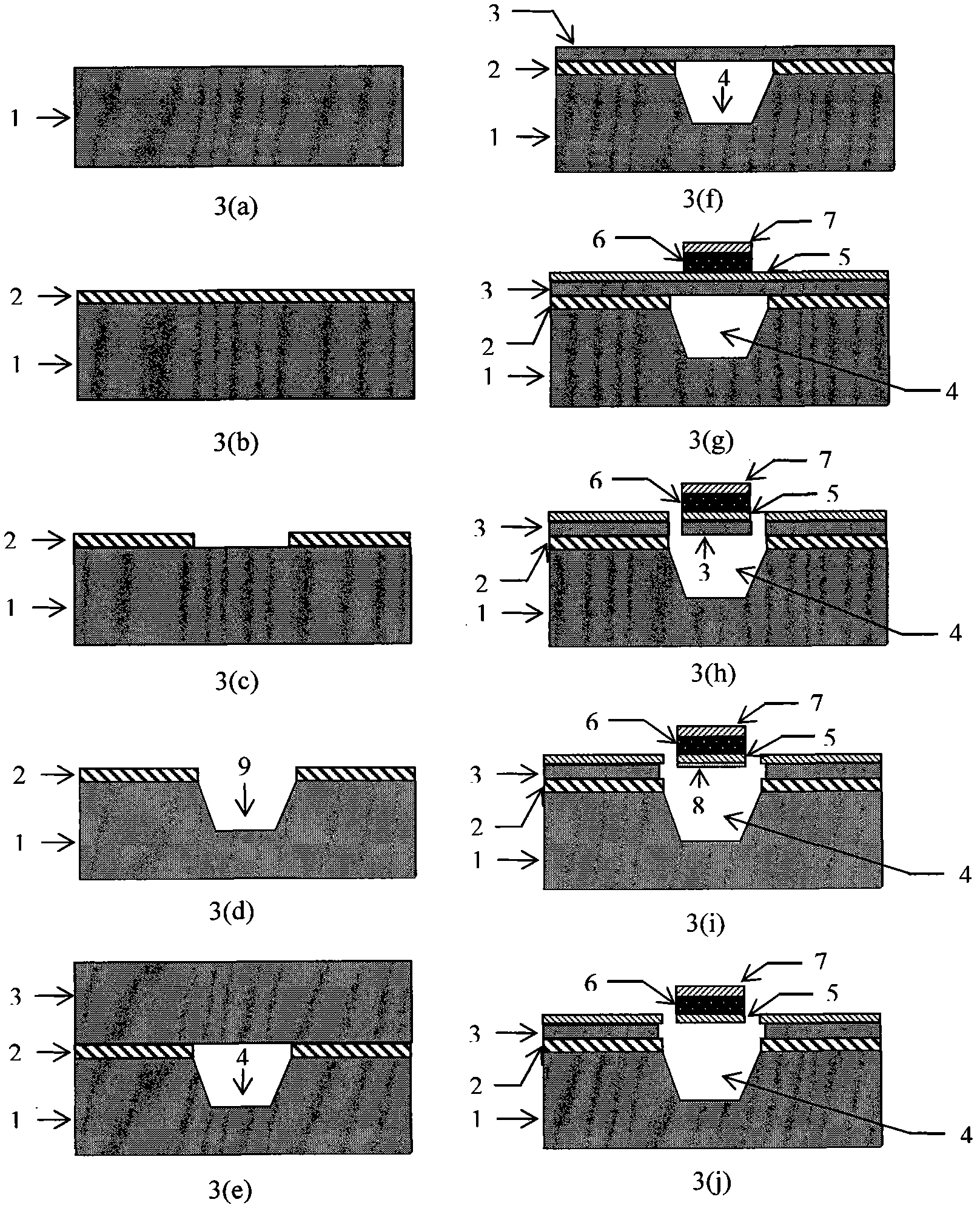
[0014] figure 1 It is a schematic diagram of the section structure of the present invention's scheme one, and the structure is composed of substrate silicon wafer 1, SiO 2 A SOI substrate with a cavity composed of layer 2, top silicon layer 3 and groove 9, and a piezoelectric thin film transducer composed of a bottom electrode layer 5, a piezoelectric thin film layer 6 and a top electrode layer 7 arranged thereon . The surface of the substrate silicon wafer 1 in the SOI substrate with a cavity is provided with grooves 9 ( image 3 Shown in (d), form a closed cavity 4 with the top layer of silicon 3 after bonding; a transducer is arranged on the top of the top layer of silicon 3, and the transducer is composed of the middle piezoelectric film 6 and the top and bottom surfaces ...


PUM

PropertyMeasurementUnit
Thicknessaaaaaaaaaa

Abstract

The invention relates to a cavity-type film bulk acoustic resonator (FBAR), consisting of a silicon on insulator (SOI) substrate with a cavity and a piezoelectric thin film transducer arranged on the substrate. The FBAR is characterized in that the surface of the substratum silicon slice in the SOI substrate with the cavity is provided with a groove, substratum silicon slice and top-layer silicon are bonded to form a closed cavity structure; the upper of the top-layer silicon is provided with a transducer which is composed of a piezoelectric thin film and thin electrodes plated on the upper surface and the lower surface of the piezoelectric thin film; and a resonator can be tuned, and the thickness of the top-layer silicon can be regulated through controlling the etching time of the top-layer silicon on the upper of the cavity, thus the resonant frequency of the resonator can be regulated. As the preset cavity structure is used, in the invention, no sacrificial layer is needed, thus the chemical mechanical polishing process and the sacrificial layer release process in aboard patents and products, which are used for treating the sacrificial layer are not required; and meanwhile, in the invention, the advantages of small source parasitic capacitance, small drain parasitic capacitance, low voltage, low power consumption and the like of an SOI material are integrated, therefore, the FBAR can be compatible with an integrated circuit (IC), is easy to integrate, has simple process and is applicable to mass production.

Description

technical field [0001] The invention relates to the field of microelectronic devices, in particular to a thin-film bulk acoustic wave resonator. Background technique [0002] Film Bulk Acoustic Resonator (FBAR) is a device that uses acoustic resonance to achieve electrical frequency selection. The basic working principle of FBAR: When an electrical signal is loaded on the FBAR, the piezoelectric film in the device converts the electrical signal into an acoustic signal through the inverse piezoelectric effect, and the specific acoustic structure of the device presents selectivity for acoustic signals of different frequencies. Realize the function of frequency regulation. [0003] The rapid development of wireless communication technology (such as mobile communication, wireless sensor network) and radar technology requires more and more high-performance integrated microwave oscillators and duplex filters, which are used in signal sources and RF front-end transceivers respecti...

Claims


Application Information

Patent Timeline
IPC IPC(8): H03H3/02
Inventor 杨增涛马晋毅江洪敏杨正兵冷俊林欧黎傅金桥赵治国张涛张龙刘积学
Owner CHINA ELECTRONICS TECH GRP NO 26 RES INST
Why Eureka
Try Eureka