Method for manufacturing large solder ball based on electroplating process
An electroplating process and solder ball technology, applied in metal material coating process, circuits, electrical components, etc., can solve the problems of difficult photoresist coating process and too large solder balls.
- Summary
- Abstract
- Description
- Claims
- Application Information
AI Technical Summary
Problems solved by technology
Method used
Image
Examples
Embodiment Construction
[0030] The present invention will be further described below in conjunction with the accompanying drawings and specific embodiments.
[0031] Such as Figure 1 to Figure 16 As shown, a method for making large solder 104 balls based on an electroplating process specifically includes the following steps:
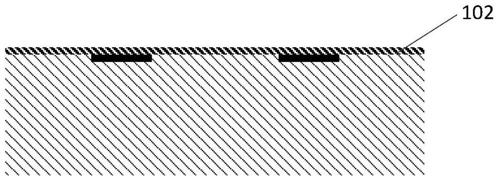
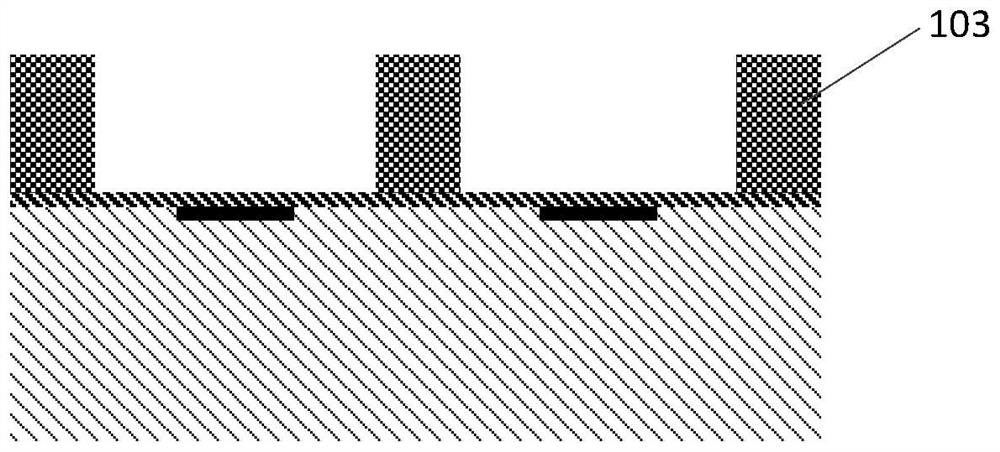
[0032] 101) Preliminary processing step: making a seed layer 102 on the upper surface of the wafer 101 by physical sputtering, magnetron sputtering or evaporation process, the thickness range of the seed layer 102 is between 1nm and 100um, and its structure is one or more Layer structure, the metal material of each layer adopts one or more mixtures of titanium, copper, aluminum, silver, palladium, gold, thallium, tin, nickel, etc. Coat the photoresist 103 on the seed layer 102, expose the plating area by developing and exposing technology, remove the seed layer 102, and plate the pad; the metal thickness of the pad ranges from 1nm to 100um, and its structure can be one layer ...
PUM
| Property | Measurement | Unit |
|---|---|---|
| thickness | aaaaa | aaaaa |
Abstract
Description
Claims
Application Information


