Manufacturing method of three-dimensional memory and three-dimensional memory manufactured by same

A manufacturing method and memory technology, applied in the direction of electric solid-state devices, semiconductor devices, electrical components, etc., can solve problems such as loss, reduce contact resistance, and affect device stability, and achieve the effect of improving process flow and stabilizing electrical properties

Active Publication Date: 2020-09-22
BEIJING E TOWN SEMICON TECH CO LTD +1
View PDF3 Cites 0 Cited by
  • Summary
  • Abstract
  • Description
  • Claims
  • Application Information

AI Technical Summary

Problems solved by technology

However, this ion implantation process requires high process stability. If process parameters fluctuate, it will easily cause the contact resistance between the channel layer of the memory cell string and the bit line contact point to be too high or too low, thus causing the entire The on-resistance of the circuit structure changes, wh

Method used


Image

  • Manufacturing method of three-dimensional memory and three-dimensional memory manufactured by same
  • Manufacturing method of three-dimensional memory and three-dimensional memory manufactured by same
  • Manufacturing method of three-dimensional memory and three-dimensional memory manufactured by same

Examples


Example Embodiment

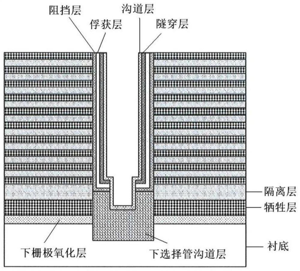
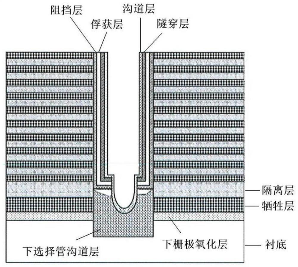
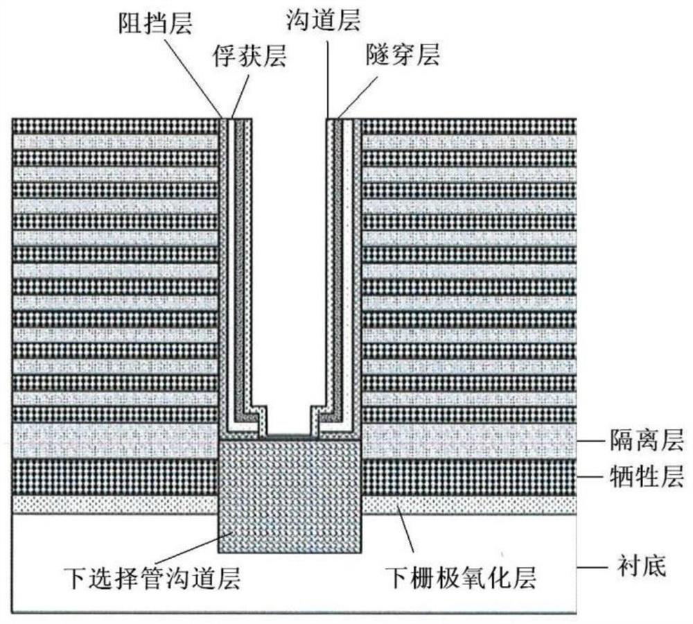
[0028] Hereinafter, some embodiments of the present disclosure will be described in detail with reference to the accompanying explanatory drawings. When referring to elements of the drawings with reference numerals, although the same elements are shown in different drawings, the same elements will be denoted by the same reference numerals. In addition, in the following description of the present disclosure, in cases where the subject matter of the present disclosure may be unclear, detailed descriptions of known functions and configurations incorporated herein will be omitted.

[0029] The terms used herein are only used for the purpose of describing specific embodiments and are not intended to limit the present disclosure. As used herein, unless the context indicates otherwise, the singular form is intended to also include the plural form. It will also be understood that the terms "including," "including," and "having" used in the specification are intended to specify the exist...


PUM


Abstract

The invention relates to a manufacturing method of a three-dimensional memory and the three-dimensional memory manufactured by the same. The manufacturing method according to the present disclosure includes the steps: forming a channel through hole in a longitudinal stack formed on a substrate, wherein the channel through hole extends from an upper layer of the longitudinal stack to the substratebelow the longitudinal stack, and the longitudinal stack is used for forming a circuit structure including an upper selection transistor, a memory cell string, and a lower selection transistor; depositing a first channel layer of the lower selection transistor on the bottom of the channel through hole; depositing a gate stack on the side wall of the channel through hole and the first channel layer; removing the gate stack on the first channel layer and a part of the first channel layer along the gate stack on the side wall of the channel through hole; depositing a second channel layer of the storage unit string in the channel through hole; and filling the channel through hole with a filling material.

Description

technical field [0001] The present disclosure relates to the technical field of semiconductor manufacturing, and more particularly, to a manufacturing method of a three-dimensional memory and a three-dimensional memory manufactured by the manufacturing method. According to the manufacturing method of the present disclosure, good ohmic contact between the channel layer of the memory cell string in the channel via hole of the three-dimensional memory and other components can be ensured. Background technique [0002] As the demand for highly integrated electronic devices continues to increase, semiconductor memory devices capable of operating at higher speeds and lower power consumption and having higher device densities are required. However, the further integration of traditional planar memories encounters bottlenecks, such as physical size limitations, development limitations of processing equipment such as photolithography machines, and electron density limitations of memor...

Claims


Application Information

Patent Timeline
IPC IPC(8): H01L27/1157H01L27/1158
CPCH10B43/23H10B43/35
Inventor 焦明洁郝志杰
Owner BEIJING E TOWN SEMICON TECH CO LTD
Why Eureka
Try Eureka