Double-gate electrode metal oxide thin film transistor and preparation method thereof

A technology of oxide thin films and oxide semiconductors, which is applied in transistors, semiconductor/solid-state device manufacturing, circuits, etc., can solve problems such as increased production costs, and achieve the effects of reduced manufacturing costs, good uniformity, and simple manufacturing processes

Inactive Publication Date: 2020-09-25
SHENZHEN CHINA STAR OPTOELECTRONICS SEMICON DISPLAY TECH CO LTD
View PDF4 Cites 2 Cited by
  • Summary
  • Abstract
  • Description
  • Claims
  • Application Information

AI Technical Summary

Problems solved by technology

Adding an additional layer of gate metal layer process will increase the production cost

Method used


Image

  • Double-gate electrode metal oxide thin film transistor and preparation method thereof

Examples


Embodiment Construction

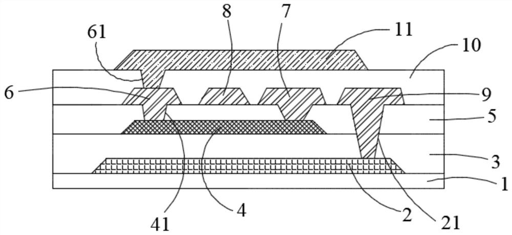
[0035] The technical solutions in the embodiments of the present application will be clearly and completely described below in conjunction with the drawings in the embodiments of the present application. Apparently, the described embodiments are only some of the embodiments of this application, not all of them. Based on the embodiments in this application, all other embodiments obtained by those skilled in the art without making creative efforts belong to the scope of protection of this application.

[0036] In the description of the present application, it should be understood that the terms "center", "longitudinal", "transverse", "length", "width", "thickness", "upper", "lower", "front", " Orientation indicated by rear, left, right, vertical, horizontal, top, bottom, inside, outside, clockwise, counterclockwise, etc. The positional relationship is based on the orientation or positional relationship shown in the drawings, which is only for the convenience of describing the a...


PUM

PropertyMeasurementUnit
thicknessaaaaaaaaaa
thicknessaaaaaaaaaa
thicknessaaaaaaaaaa

Abstract

The invention discloses a double-gate electrode metal oxide thin film transistor and a preparation method thereof. The double-gate electrode metal oxide thin film transistor comprises a substrate; a bottom gate electrode, a bottom gate insulating layer, a metal oxide semiconductor layer and a passivation layer sequentially arranged on the substrate, and a source electrode, a drain electrode, a first top gate electrode and a second top gate electrode arranged on the passivation layer; a flat layer and a pixel electrode layer. The source electrode, the drain electrode, the first top gate electrode and the second top gate electrode are located on the same layer, and the second top gate electrode is connected with the bottom gate electrode through a bottom gate electrode contact hole. The topgate electrode, the source electrode and the drain electrode are made of the same layer of metal, the top gate and the bottom gate are in signal communication to form the double-gate structure device,the process is simple, and the cost is saved.

Description

technical field [0001] The present application relates to the technical field of displays, in particular to a double-gate metal oxide thin film transistor and a preparation method thereof. Background technique [0002] As the core device of active matrix drive flat panel display technology, thin film transistors are widely used in the display field. At present, in flat panel display technology, silicon-based thin film transistor (Thin Film Transistor, TFT for short) is a relatively mature industrialized technology, mainly including amorphous silicon TFT and polysilicon TFT. With the development of flat panel display technology in the direction of large area, high resolution, flexible and rollable type and the emergence of many new flat panel display technologies, higher requirements are put forward for the performance of TFT. In recent years, TFTs with amorphous metal oxide semiconductors as active layers have become the focus of research due to their excellent performance....

Claims


Application Information

Patent Timeline
Patent Type & Authority Applications(China)
IPC IPC(8): H01L29/786H01L21/34
CPCH01L29/66969H01L29/78645H01L29/78648H01L29/78693
Inventor 周星宇
Owner SHENZHEN CHINA STAR OPTOELECTRONICS SEMICON DISPLAY TECH CO LTD
Why Eureka
Try Eureka