Multi-beam millimeter wave phased array chip and manufacturing method

A millimeter wave and phased array technology, which is applied in the field of multi-beam millimeter wave phased array chips and manufacturing, can solve the problems that beamforming chips are difficult to realize, and achieve array layout, reduce area and cost, and reduce power consumption. consumption effect

Active Publication Date: 2020-09-29
中国星网网络应用有限公司
View PDF7 Cites 9 Cited by
  • Summary
  • Abstract
  • Description
  • Claims
  • Application Information

AI Technical Summary

Problems solved by technology

For large-scale phased arrays with wideband frequency / polarization multiplexing, multi-beam, and wideband scanning requirements, beamforming chips are more important but difficult to implement

Method used


Image

  • Multi-beam millimeter wave phased array chip and manufacturing method
  • Multi-beam millimeter wave phased array chip and manufacturing method
  • Multi-beam millimeter wave phased array chip and manufacturing method

Examples


Embodiment Construction

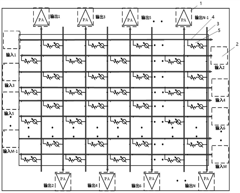
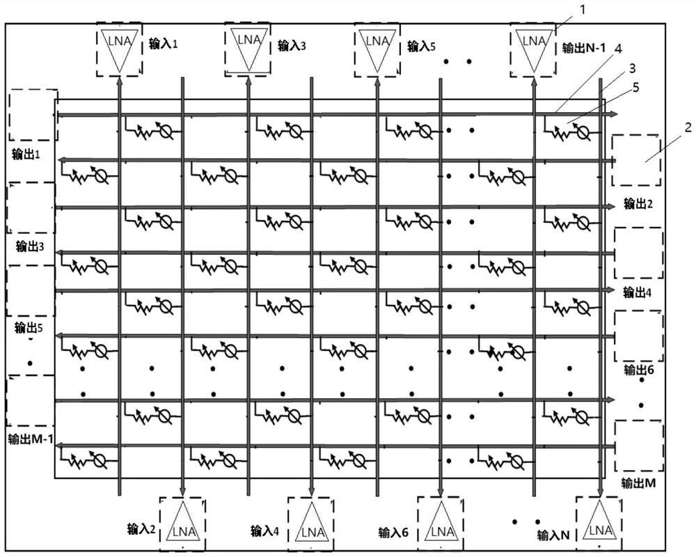
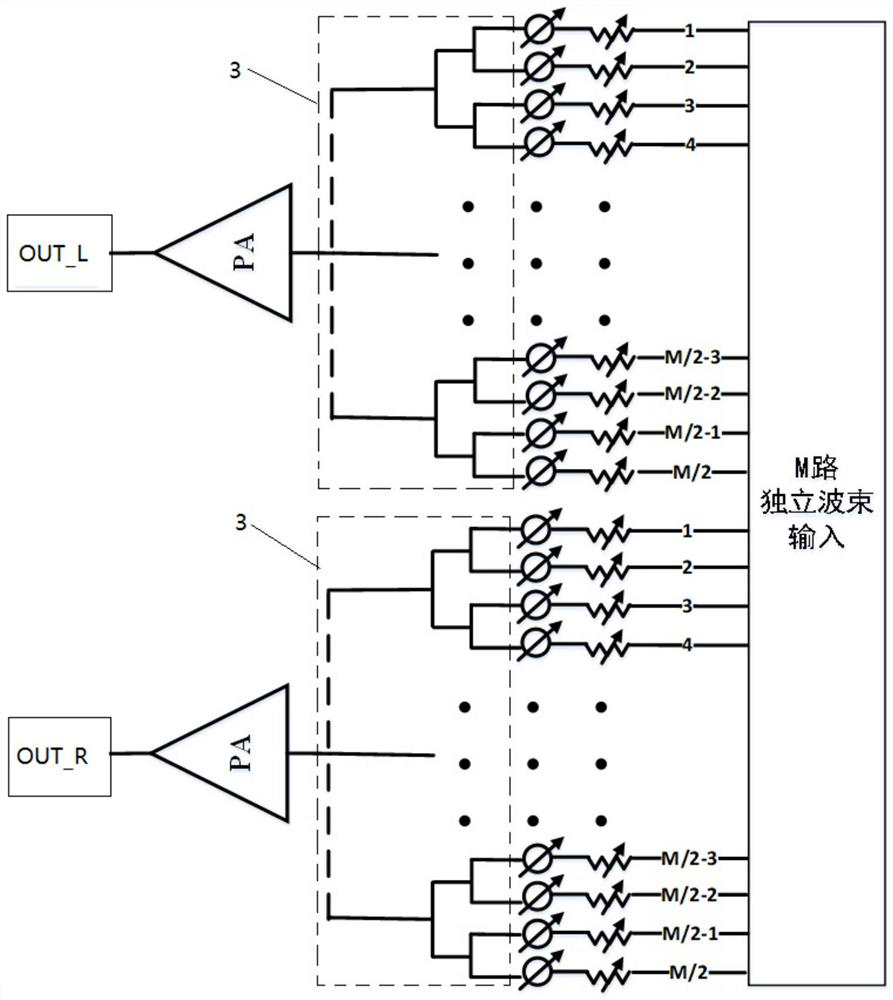
[0031] Embodiments of the present invention are described in detail below, examples of which are shown in the drawings, wherein the same or similar reference numerals designate the same or similar elements or elements having the same or similar functions throughout. The embodiments described below by referring to the figures are exemplary only for explaining the present invention and should not be construed as limiting the present invention.

[0032] In describing the present invention, it should be understood that the terms "longitudinal", "transverse", "upper", "lower", "front", "rear", "left", "right", "vertical", The orientation or positional relationship indicated by "horizontal", "top", "bottom", "inner", "outer", etc. are based on the orientation or positional relationship shown in the drawings, and are only for the convenience of describing the present invention and simplifying the description, rather than Nothing indicating or implying that a referenced device or elem...


PUM


Abstract

The invention discloses a multi-beam millimeter wave phased array chip and a manufacturing method. The chip comprises N antenna connecting ends, N reversible first couplers, a plurality of phase shiftattenuators, M reversible second couplers and M signal connecting ends, k polarization direction wave beams of the frequencies are transmitted to M signal connecting ends, and the signal connecting ends are connected with the first ends of the second couplers in a one-to-one correspondence mode; the N first couplers are divided into K groups, and each group transmits a polarization direction wavebeam; a phase shift attenuator is connected between the second end of the first coupler and the second end of the second coupler on the beam transmission channel in the same polarization direction; when the chip is a transmitting chip, the chip also comprises N power amplifiers; and when the chip is a receiving chip, the chip also comprises N low-noise amplifiers. Different carrier frequency beams in the same polarization direction share the same power amplifier or the same low-noise amplifier corresponding to the array element, the number of the power amplifiers or the low-noise amplifiers is reduced, and the integration level of the phased array chip is improved.

Description

technical field [0001] The invention relates to the technical field of integrated circuits, in particular to a multi-beam millimeter-wave phased array chip and a manufacturing method. Background technique [0002] Millimeter-wave band signals have short wavelength and large attenuation, but at the same time, the beam is narrow and has good directivity, which complements the characteristics of phased arrays that are easy to realize beam scanning and beam forming. Therefore, millimeter-wave communication usually uses phased array technology to obtain high-quality Efficient isotropic radiated power (EIRP), high antenna gain temperature-to-noise ratio (G / T), wide beam scanning, and good beam characteristics. [0003] Millimeter-wave phased array communication still faces problems such as difficult design, complex system, high cost, high power consumption, difficulty in heat dissipation, and difficulty in array layout. These technical challenges and limitations have greatly affec...

Claims


Application Information

Patent Timeline
Patent Type & Authority Applications(China)
IPC IPC(8): G01S7/02H03F1/26H03F3/20
CPCG01S7/026H03F3/20H03F1/26Y02D30/70
Inventor 邹光南朱进宇王艳峰
Owner 中国星网网络应用有限公司
Why Eureka
Try Eureka