A heat dissipation substrate, power module, power device and heat dissipation substrate processing method
A heat dissipation substrate and power module technology, which is applied in the manufacture of semiconductor devices, electrical solid state devices, semiconductor/solid state devices, etc., can solve the problems of heat dissipation, heat dissipation, and conduction of power chips, and achieve low assembly difficulty and low processing cost Effect
- Summary
- Abstract
- Description
- Claims
- Application Information
AI Technical Summary
Problems solved by technology
Method used
Image
Examples
Embodiment 1
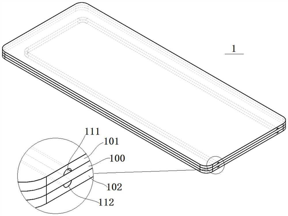
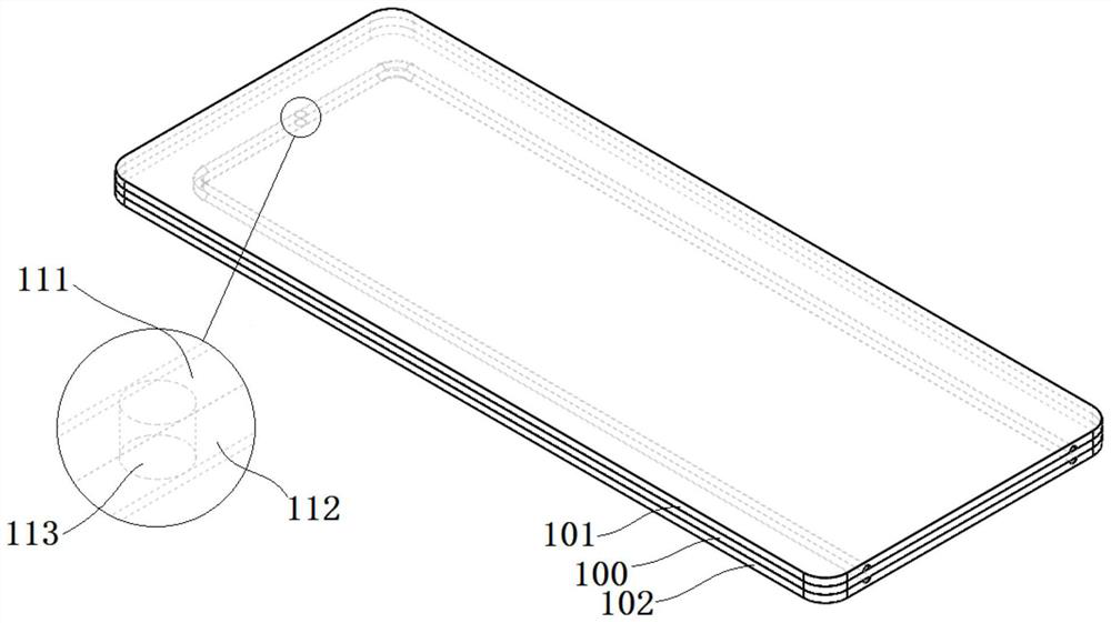
[0051] figure 1 A schematic diagram of a three-dimensional perspective structure of a heat dissipation substrate according to an embodiment of the present invention is shown. The present invention provides a heat dissipation substrate 1, basically, the heat dissipation substrate 1 includes a first conductive surface layer 101, a connection layer 100 and a second conductive surface layer 102, specifically, the first conductive surface layer 101 and the second conductive surface layer 102 are electrically connected, and the potentials of the first conductive surface layer 101 and the second conductive surface layer 102 are equal everywhere.
[0052] Specifically, the first conductive surface layer 101 and the second conductive surface layer 102 are attached to the two surfaces of the connection layer 100 respectively, and the three are combined to form the heat dissipation substrate 1 .
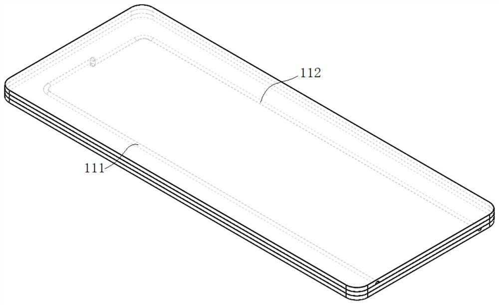
[0053] Specifically, a first flow channel 111 is provided between the first conductive surfa...
Embodiment 2
[0059] Specifically, the manner in which the first conductive surface layer 101 and the second conductive surface layer 102 are electrically connected includes: the connection layer 100 is an insulating layer, and the first conductive surface layer 101 and the second conductive surface layer 102 are based on passing through The electrical connectors or copper sink holes of the connection layer are electrically connected; or the connection layer 100 is a conductive layer, and the first conductive surface layer 101 and the second conductive surface layer 102 are electrically connected based on the connection layer.
[0060] In a specific implementation, the entire heat dissipation substrate 1 can be regarded as a whole metal plate, the electric potentials of the heat dissipation substrate 1 are equal everywhere, and the whole heat dissipation substrate 1 can be regarded as a large electrode. Through this embodiment, the embodiment of the electrical connection between the first co...
Embodiment 3
[0062] Optionally, the first flow channel 111 is disposed on the first conductive surface layer 101 ; and / or the second flow channel 112 is disposed on the second conductive surface layer 102 .
[0063] The above arrangement of the first flow channel and the second flow channel mainly considers the convenience of processing, especially when the heat dissipation substrate 1 is a DBC substrate structure, it can avoid processing on the connection layer with poor processability, and has good processing convenience.
PUM
 Abstract
Description
Claims
Application Information


