Data-outputting buffer circuit
A technology for output buffering and data, applied in the direction of logic circuit connection/interface layout, electrical components, electronic switches, etc., can solve the problems of pull-up operation delay, impossible to effectively suppress noise, delay charge accumulation time, etc.
- Summary
- Abstract
- Description
- Claims
- Application Information
AI Technical Summary
Problems solved by technology
Method used
Image

Examples
Embodiment Construction
[0021] The preferred embodiments of the present invention will now be described in detail, examples of which are given in the accompanying drawings.
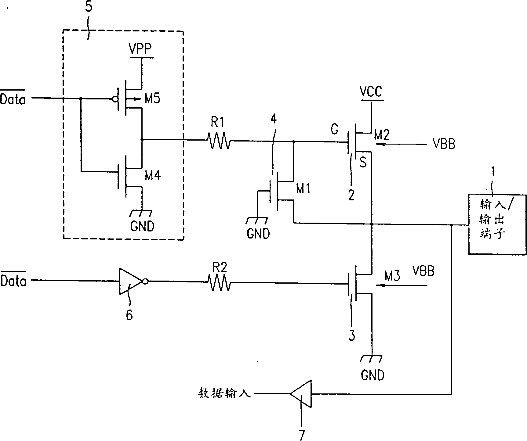
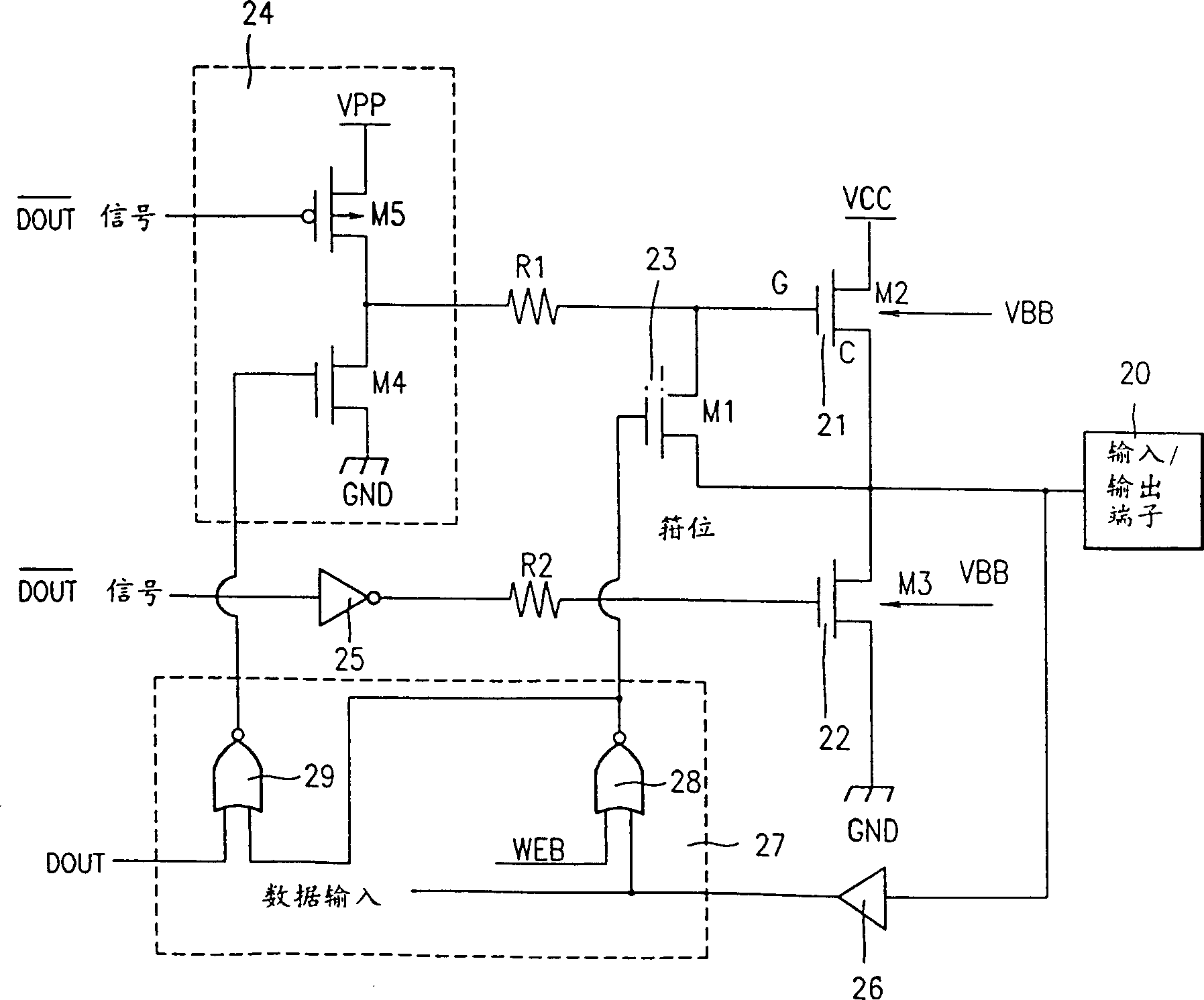
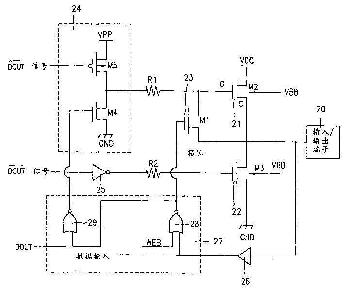
[0022] A data output buffer circuit includes a pull-up transistor 21 and a pull-down transistor 22, the two transistors are connected in series with each other through their sources, and the two sources are commonly connected to the input / output terminal 20; a noise generation suppressing section 27 , used to logically operate the data signal and the write enable signal WEB to generate a noise suppression signal; a clamping transistor 23 having a gate connected to the noise generation suppression portion 27 and the gate of the pull-up transistor 21; a first A driving part 24 includes PMOS M5 and NMOS M4 connected in series with each other, and is connected to the gate of the pull-up transistor 21 through a noise reduction resistor R1 to drive the pull-up transistor 21; a second driving part 25, through A noise reducing resistor ...
PUM
 Abstract
Description
Claims
Application Information
 - R&D
- Intellectual Property
- Life Sciences
- Materials
- Tech Scout
- Unparalleled Data Quality
- Higher Quality Content
- 60% Fewer Hallucinations
Browse by: Latest US Patents, China's latest patents, Technical Efficacy Thesaurus, Application Domain, Technology Topic, Popular Technical Reports.
© 2025 PatSnap. All rights reserved.Legal|Privacy policy|Modern Slavery Act Transparency Statement|Sitemap|About US| Contact US: help@patsnap.com