FPGA device of network-on-chip is formed using silicon connection layer

An on-chip network and connection layer technology, applied in the FPGA field, can solve problems such as difficult promotion, difficult production, and chip area occupation, and achieve the effect of efficient interconnection and communication

Active Publication Date: 2020-10-09
WUXI ESIONTECH CO LTD
View PDF9 Cites 4 Cited by
  • Summary
  • Abstract
  • Description
  • Claims
  • Application Information

AI Technical Summary

Problems solved by technology

With the increasing demand for bandwidth, storage and data processing capabilities of new applications, there are currently some ways to integrate NOC networks inside FPGA chips to improve communication performance, but the production is difficult and difficult to promote at present, and this method will take up precious resources. chip area

Method used


Image

  • FPGA device of network-on-chip is formed using silicon connection layer
  • FPGA device of network-on-chip is formed using silicon connection layer
  • FPGA device of network-on-chip is formed using silicon connection layer

Examples


Embodiment Construction

[0026] The specific embodiments of the present invention will be further described below in conjunction with the accompanying drawings.

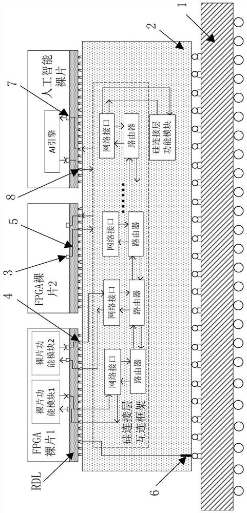
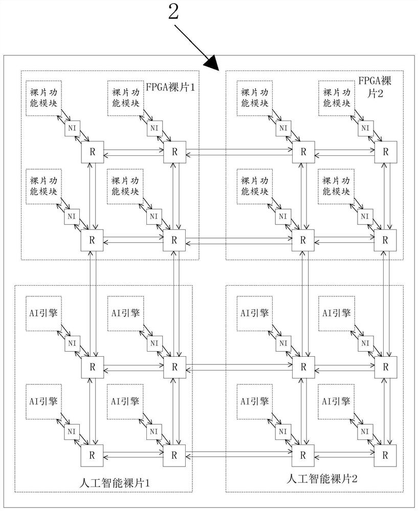
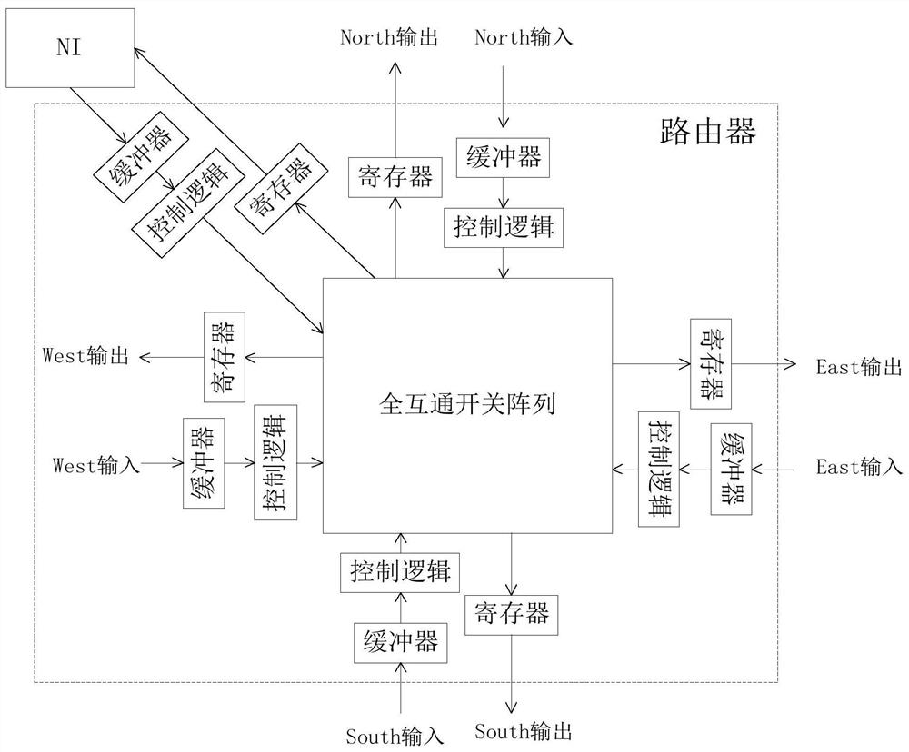
[0027] This application discloses an FPGA device that uses a silicon connection layer to form an on-chip network. Please refer to figure 1 , the FPGA device includes a substrate 1, a silicon connection layer 2, and an FPGA die that are sequentially stacked from bottom to top. Protect the packaging shell of each component, and also include the pins connected to the substrate for signal extraction, etc., figure 1 These conventional structures are not shown in detail.

[0028] The FPGA bare chip in this application is different from the conventional FPGA bare chip. The conventional FPGA bare chip mainly includes CLB, PLBs, BRAM, DSP, PC, IOB and other bare chip functional modules. Each bare chip functional module has a Interconnect resource modules (INT) distributed around the bare chip functional modules with the same structure, and the hori...


PUM


Abstract

The invention discloses an FPGA device for forming a network-on-chip by using a silicon connection layer, relating to the technical field of FPGA. An active silicon connection layer is designed in theFPGA device. A silicon connection layer interconnection frame is arranged in the silicon connection layer, and each bare chip function module in the FPGA bare chip is accessed to the silicon connection layer interconnection framework to form an on-chip network together with the silicon connection layer interconnection framework; each bare chip function module, a network interface in the silicon connection layer interconnection framework and the router form an NOC node; and the NOC nodes are communicated with each other, so that the bare chip function modules in the FPGA bare chip without thebuilt-in NOC network can be efficiently interconnected and communicated through the silicon connection layer interconnection framework, and the processing difficulty is reduced on the basis of improving the data transmission bandwidth and performance in the FPGA device.

Description

technical field [0001] The invention relates to the field of FPGA technology, in particular to an FPGA device which utilizes a silicon connection layer to form an on-chip network. Background technique [0002] FPGA (Field Programmable Gate Array, Field Programmable Logic Gate Array) is a hardware programmable logic device, which is widely used in mobile communication, data center, navigation guidance and automatic driving and other fields. With the increasing demand for bandwidth, storage and data processing capabilities of new applications, there are currently some ways to integrate NOC networks inside FPGA chips to improve communication performance, but the production is difficult and difficult to promote at present, and this method will take up precious resources. chip area. Contents of the invention [0003] The present inventor proposes a kind of FPGA device that utilizes silicon connection layer to form network-on-chip for above-mentioned problem and technical deman...

Claims


Application Information

Patent Timeline
Patent Type & Authority Applications(China)
IPC IPC(8): H01L25/18H01L25/00H01L23/535H01L23/538G06F30/34
CPCH01L25/18H01L25/50H01L23/535H01L23/5386G06F30/34H03K19/17736H01L25/0655H01L2224/16225H01L2924/15311H01L24/16H01L25/0652H01L2224/16146H01L2224/16227H01L2224/16238H01L2924/1431H01L2924/14361G06F30/394G06F30/39H03K19/17744G06F15/7825G06F30/347H10B80/00
Inventor 范继聪徐彦峰单悦尔闫华张艳飞
Owner WUXI ESIONTECH CO LTD
Why Eureka
Try Eureka