Medium-wave double-color infrared detector
An infrared detector and two-color technology, applied in the field of infrared detectors, can solve the problems of long calculation time and consumption, and achieve the effect of reducing power consumption
- Summary
- Abstract
- Description
- Claims
- Application Information
AI Technical Summary
Problems solved by technology
Method used
Image
Examples
Embodiment 1
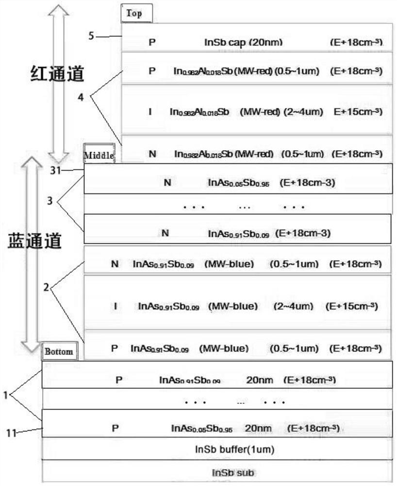
[0026] The first embodiment of the present invention provides a medium-wave two-color infrared detector, such as figure 1 As shown, it includes: a substrate, a first PIN structure 2 and a second PIN structure 4;
[0027] Wherein, the first PIN structure 2 is grown on the substrate, and the second PIN structure 4 and the first PIN structure 2 are stacked back to back.
[0028] Specifically, in this embodiment, a commercial direct epitaxial (Epi-ready) N-type InSb (100) substrate can be selected for the substrate InSb sub, and the substrate is pretreated and completely deoxidized in the MBE equipment. Then the first PIN structure 2 and the second PIN structure 4 are grown on the substrate InSb sub, wherein as figure 1 As shown, the first PIN structure 2 and the second PIN structure 4 are stacked back to back. The two-color infrared detector of the present invention realizes medium-wave two-color detection and reduces the power consumption, volume, weight and cost of the detecto...
Embodiment 2
[0054] The second embodiment of the present invention provides a method for manufacturing a medium-wave two-color infrared detector, which includes the following specific steps:
[0055] The commercial direct epitaxial (Epi-ready) N-type InSb (100) substrate is selected, and the substrate is pretreated and completely deoxidized in the MBE equipment. Epitaxial growth of the medium-wave two-color infrared detector structure according to the following steps:
[0056] 1. Epitaxial growth of 1 μm thick non-doped InSb buffer buffer layer;
[0057] 2. Epitaxially grow T (T≥3) 20nm thick P-type (10 18 cm -3 )InAs 1-x Sb x Component gradient buffer layer, from InAs 0.05 Sb 0.95 until InAs 0.91 Sb 0.09 , T is as large as possible to provide a lattice-matched gradient buffer layer;
[0058] 3. Epitaxial growth of 0.5-1μm thick P-type (10 18 cm -3 )InAs 0.91 Sb 0.09 MW blue channel electrode layer;
[0059] 4. Epitaxial growth of 2-4μm thick non-doped InAs 0.91 Sb 0.09 MW ...
PUM
| Property | Measurement | Unit |
|---|---|---|
| thickness | aaaaa | aaaaa |
| thickness | aaaaa | aaaaa |
| thickness | aaaaa | aaaaa |
Abstract
Description
Claims
Application Information
