Mainboard repairing method

A motherboard and repair technology, applied in manufacturing tools, electrical solid devices, laser welding equipment, etc., can solve problems such as low alignment accuracy, damage, abnormal pressure, etc., to achieve high repair efficiency, good adaptability, and small thermal impact. Effect

Active Publication Date: 2020-10-16
深圳市微组半导体科技有限公司
View PDF7 Cites 4 Cited by
  • Summary
  • Abstract
  • Description
  • Claims
  • Application Information

AI Technical Summary

Problems solved by technology

Due to the large size and the large number of miniLEDs and miniICs, it is impossible to complete the repair manually, and supporting technology and equipment must be used to solve this problem
[0005]MiniLED backlight circuit boards often have defective or damaged MiniLED lamp bead chips and MiniIC chips in the process of manufacturing. Short circuit and open circuit caused by poor solder and soldering temperature, bad soldering caused by abnormal solder and soldering temperature, quality problems of the device itself, damage caused by abnormal pressure in the device placement process, etc., need to be repaired by using this application to improve yield and reduce production cost
[0006]The traditional hot air heating rework station in the SMT industry uses the following methods to repair PCB circuit board faults: alignment—heating—removal—soldering. The limitations of this type of method are as follows : Low alignment accuracy, large rework target size, poor heating range control, unsatisfactory protection for chips / PCB boards, unable to perform surgical scalpel-style precise rework on a single defective IC
[0007] The size of the rework target (MiniLED lamp bead and MiniIC chip) of this application is developing in the direction of miniaturization. For the size (typical value 4*6mil), the accuracy (typical value 10um@3sigma), and the requirements for the heat-affected zone are very strict. In view of the fact that the hot air rework station cannot meet these performance requirements well, a bare Die rework technology for MiniLED and MiniIC is hereby developed

Method used


Image

  • Mainboard repairing method
  • Mainboard repairing method

Examples


Embodiment Construction

[0028] In order to have a clearer understanding of the technical features, purposes and effects of the present invention, the specific implementation manners of the present invention will now be described in detail with reference to the accompanying drawings.

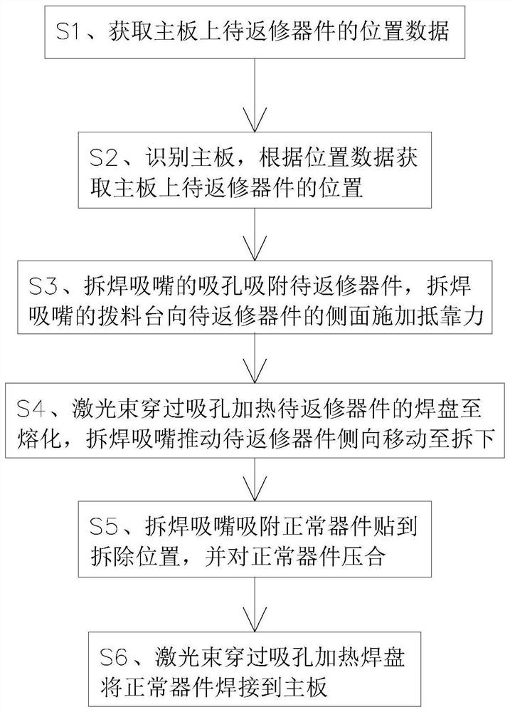
[0029] Such as figure 1 , figure 2 As shown, the motherboard repairing method in a preferred embodiment of the present invention comprises the following steps:

[0030] S1. Obtain the position data of the device 2 to be repaired on the main board 1;

[0031] S2. Identify the main board 1, and obtain the position of the device 2 to be repaired on the main board 1 according to the position data;

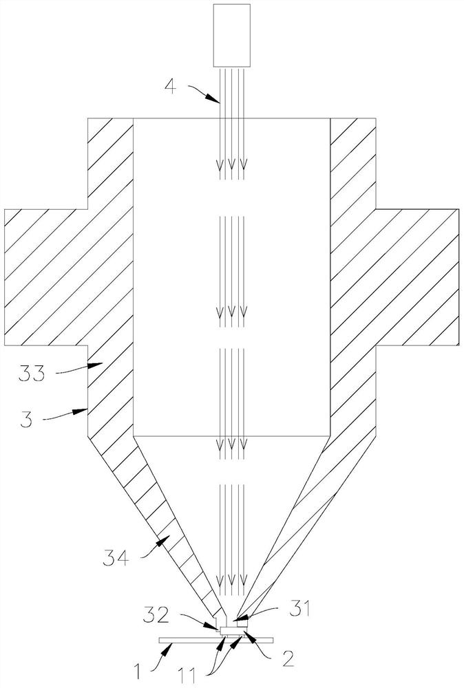
[0032] S3. The light-transmitting hole 31 of the desoldering nozzle 3 absorbs the device 2 to be repaired, and the material pushing table 32 of the desoldering nozzle 3 applies an abutting force to the side of the device 2 to be repaired;

[0033] S4. The laser beam 4 passes through the light transmission hole 31 to heat the...


PUM


Abstract

The invention relates to a mainboard repairing method. The mainboard repairing method comprises the following steps: S1, acquiring position data of a to-be-repaired device on a mainboard; S2, identifying the mainboard, and obtaining the position of the to-be-repaired device on the mainboard according to the position data; S3, enabling a light hole of a desoldering suction nozzle to adsorb the to-be-repaired device, and enabling a material stirring table of the desoldering suction nozzle to apply an abutting force to the side face of the to-be-repaired device; S4, enabling a laser beam to passthrough the light hole to heat a bonding pad of the to-be-repaired device until the bonding pad is molten, and enabling the desoldering suction nozzle to push the to-be-repaired device to move laterally until the to-be-repaired device is dismounted; S5, enabling the desoldering suction nozzle to suck the normal device to be attached to the desoldering position, and pressing the normal device; S6,enabling the laser beam to pass through the light hole to heat the bonding pad to weld the normal device to the mainboard. When the repair technology is used for repairing damaged lamp beads or Mini IC chips on the Mini LED backlight mainboard to wait for repair devices, the repair efficiency is high, the precision is high, the adaptability to small and micro devices is good, the heat influence issmall, no damage is caused to a repair target, and the high yield of products is ensured.

Description

technical field [0001] The invention relates to the field of mainboard processing, and more specifically, relates to a method for repairing a mainboard. Background technique [0002] As we all know, Mini / Micro LED has excellent performance and is expected to become a new trend of LED display. LCD display using Mini LED backlight technology is superior to current LCD displays in terms of brightness, contrast, color reproduction and energy saving, and can even compete with AMOLED. Control production costs. [0003] Technological progress drives Mini LED to be upgraded as a small-pitch display product. As an extension of small-pitch technology, Mini LED is expected to usher in application penetration in the field of commercial and home display. [0004] At present, major domestic display panel manufacturers are actively developing and putting into production lines to produce 65-inch full-panel, 75-inch double-panel and 110-inch miniLED multi-zone backlight displays. Due to t...

Claims


Application Information

Patent Timeline
Patent Type & Authority Applications(China)
IPC IPC(8): H01L27/15H01L33/48B23K26/00B23P6/00
CPCH01L33/48H01L27/15B23P6/00B23K26/00H01L2933/0033
Inventor 王文林佛迎
Owner 深圳市微组半导体科技有限公司
Why Eureka
Try Eureka