Spiro benzoanthracene-fluorene derivatives and their use in organic electronic devices, displays and lighting devices

A technology of organic electronic devices and electron transport layers, applied in lighting devices, organic semiconductor devices, electric solid devices, etc., can solve problems such as disturbing charge carrier mobility and reducing device performance

Pending Publication Date: 2020-10-16
NOVALED GMBH
View PDF9 Cites 4 Cited by
  • Summary
  • Abstract
  • Description
  • Claims
  • Application Information

AI Technical Summary

Problems solved by technology

However, bulky molecular fragments can significantly interfere with charge carrier mobility, thereby degrading overall device performance

Method used


Image

  • Spiro benzoanthracene-fluorene derivatives and their use in organic electronic devices, displays and lighting devices
  • Spiro benzoanthracene-fluorene derivatives and their use in organic electronic devices, displays and lighting devices
  • Spiro benzoanthracene-fluorene derivatives and their use in organic electronic devices, displays and lighting devices

Examples


Embodiment Construction

[0218] Reference will now be made in detail to the exemplary embodiments of the present invention, examples of which are illustrated in the accompanying drawings, wherein like reference numerals refer to like elements throughout. The exemplary embodiments are described below, by referring to the figures, in order to explain aspects of the present invention.

[0219] Here, when a first element is referred to as being formed or disposed "on" or "over" a second element, the first element may be directly disposed on the second element, or one or more other elements may be disposed on the first element. element and the second element. When a first element is referred to as being "directly formed or disposed on" or "directly formed or disposed on" a second element, there are no other elements interposed between the first element and the second element.

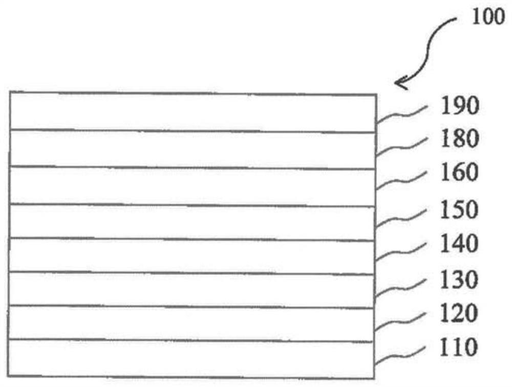
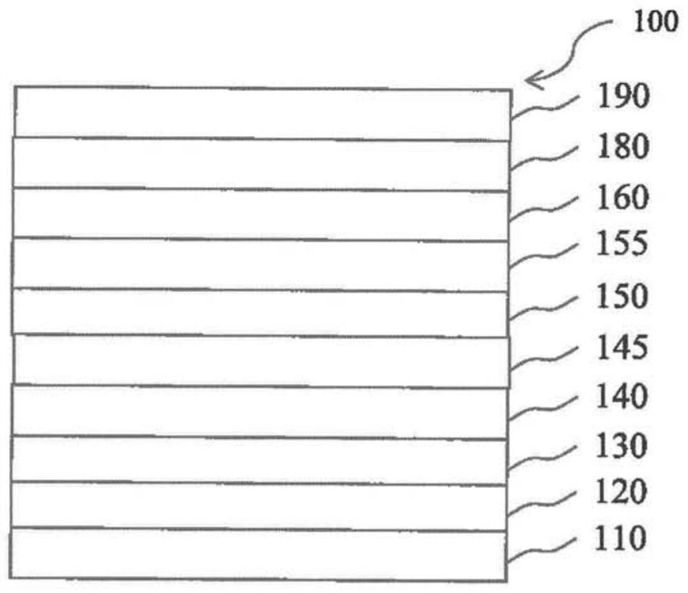
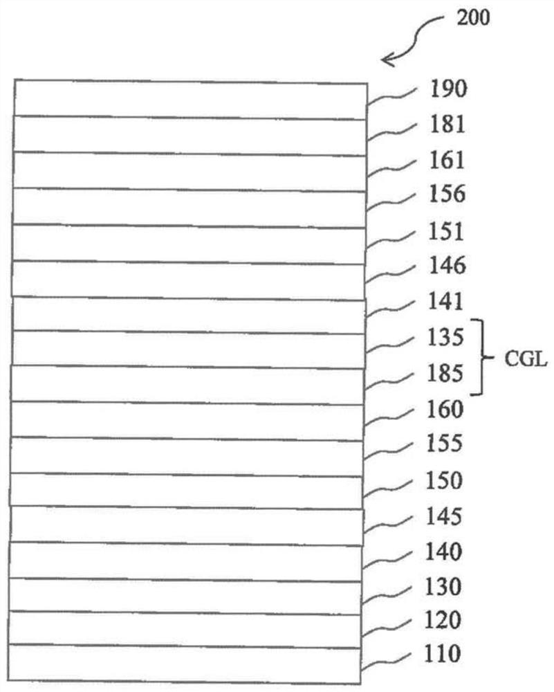
[0220] figure 1 is a schematic cross-sectional view of an organic light emitting diode (OLED) 100 according to an exemplary emb...


PUM

PropertyMeasurementUnit
thicknessaaaaaaaaaa
thicknessaaaaaaaaaa
thicknessaaaaaaaaaa

Abstract

The present invention relates to an organic electronic device comprising, between an anode and a cathode, at least one layer selected from an electron injection layer, an electron transport layer or an electron generation layer, the layer comprising at least one compound of the following Formula (I), wherein the compound of Formula (I) comprises one or more moieties -(A)a-L and the remaining positions marked with * are hydrogen or substituents independently selected from the group consisting of deuterium, fluorine, RF, C1-C20 linear alkyl, C3-C20 branched alkyl, C1-C12 linear fluorinated alkyl, CN, RCN, C6-C20 aryl, C2-C20 heteroaryl, (P=O)R2; each R is independently selected from C1-C20 linear alkyl, C1-C20 alkoxy, C1-C20 thioalkyl, C3-C20 branched alkyl, C3-C20 cyclic alkyl, C3-C20 branched alkoxy, C3-C20 cyclic alkoxy, C3-C20 branched thioalkyl, C3-C20 cyclic thioalkyl, C6-C20 aryl and C2-C20 heteroaryl; A is selected from substituted or unsubstituted C6-C24 aryl or C2-C20 heteroaryl; in case that A is substituted, the respective substituents are independently selected from the group consisting of deuterium, fluorine, C1-C20 linear alkyl, C3-C20 branched alkyl, linear fluorinated C1-C12 alkyl, CN, C6-C20 aryl, and C2-C20 heteroaryl; L is selected from substituted or unsubstituted C2-C42 heteroaryl, substituted or unsubstituted C6-C24 aryl or a polar group selected from (formula (aa)), (formula (bb)) and (formula (cc)), wherein substituents, if present in the respective group L are independently selected from the group consisting of deuterium, fluorine, C1-C20 linear alkyl, C3-C20 branched alkyl, C3-C20 cyclic alkyl, C1-C20 linear alkoxy, C3-C20 branched alkoxy, C1-C12 linear fluorinated alkyl, C1-C12 linear fluorinated alkoxy, C3-C12 branched fluorinated cyclic alkyl, C3-C12 fluorinated cyclic alkyl, C3-C12 fluorinated cycle alkoxy, CN, RCN, C6-C20 aryl, C2-C20 heteroaryl, OR, SR, (C=O)R, (C=O)NR2, SiR3, (S=O)R (S=O)2R, (P=O)R2; each R independenfly selected fromC1-C20 linear alkyl, C1-C20 alkoxy, C1-C20 thioalkyl, C3-C20 branched alkyl, C3-C20 cyclic alkyl, C3-C20 branched alkoxy, C3-C20 cyclic alkoxy, C3-C20 branched thioalkyl, C3-C20 cyclic thioalkyl, C6-C20 aryl and C2-C20 heteroaryl, and a is an integer from o to 2, respective compounds as well as display and lightning devices comprising the same.

Description

technical field [0001] The present invention relates to an organic electronic device, a compound that can be included in the organic electronic device, an organic semiconductor layer including the compound, and a display or lighting device including the organic electronic device. Background technique [0002] Organic Light Emitting Diodes (OLEDs) are self-luminous devices with wide viewing angles, excellent contrast, fast response, high brightness, excellent driving voltage characteristics, and color reproduction. A typical OLED includes an anode, a hole transport layer (HTL), an emission layer (EML), an electron transport layer (ETL) and a cathode sequentially stacked on a substrate. In this regard, the HTL, EML and ETL layers are thin films formed of organic and / or organometallic compounds. [0003] When a voltage is applied to the anode and the cathode, holes injected from the anode move to the EML through the HTL, and electrons injected from the cathode move to the EML ...

Claims


Application Information

Patent Timeline
Patent Type & Authority Applications(China)
IPC IPC(8): C07C255/50C07D215/06C07D221/12C07D221/18C07D333/50C07D235/18C07D239/26C07D251/24C07D471/04C07C233/65C07D263/57C07D277/66C07D213/06C07D307/77C07D307/91C09K11/06H01L51/00H05B33/14
CPCC07C233/64C07C255/50C07C2603/94C07D213/16C07D215/04C07D221/12C07D221/18C07D235/18C07D239/26C07D251/24C07D263/57C07D277/66C07D307/92C07D333/76C07D405/04C07D471/04C07C233/65C07D213/06C07D215/06C07D307/77C07D307/91C07D333/50C09K11/06H05B33/14H10K99/00H10K85/625H10K85/622H10K85/615H10K85/654H10K85/6574H10K50/165H10K50/00C09K2211/1007C09K2211/1011C09K2211/1059H10K50/18H10K50/16H10K85/626H10K85/6576H10K30/353H10K50/11H10K50/156H10K50/166H10K50/171H10K2101/30H10K2101/40
Inventor 利迪亚·马林伊莱纳·加兰
Owner NOVALED GMBH
Why Eureka
Try Eureka