

Semiconductor laser
A laser and semiconductor technology, which is applied in the direction of semiconductor lasers, lasers, laser components, etc., can solve problems such as technical issues are not very clear, and achieve the effects of suppressing light absorption loss, reducing Auger loss, and decreasing threshold current density
Inactive Publication Date: 2003-08-13
NIPPON SANSO CORP
View PDF4 Cites 1 Cited by
- Summary
- Abstract
- Description
- Claims
- Application Information
AI Technical Summary
Problems solved by technology
[0005] However, the existing research and development of semiconductor lasers in this material series are almost all focused on the wavelength bands of 1.3 μm and 1.55 μm, and the design of lasers with wavelengths longer than 1.6 μm is mostly used as it is 1.3 μm and 1.55 μm The current situation is that the technical issues in this area are still not very clear
Method used
View moreImage
Smart ImageViewing Examples

Examples
Embodiment 1
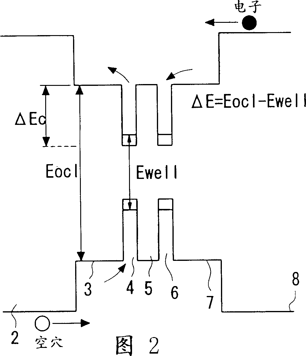
[0041] Sample B with ΔE set at 278meV has an external differential efficiency of 34.5% and a characteristic temperature of 43°K. Good laser characteristics can be obtained.
Embodiment 2
[0043] Set ΔE as sample C of 299meV, due to the large amount of strain, the film thickness of the strained quantum well is close to the critical film thickness, and the external differential efficiency is 27%. Compared with Example 1, the external differential efficiency is low, but the characteristic temperature Roughly equal. In addition, the operating temperature has less influence on the external differential efficiency.
Login to View More PUM
 Abstract
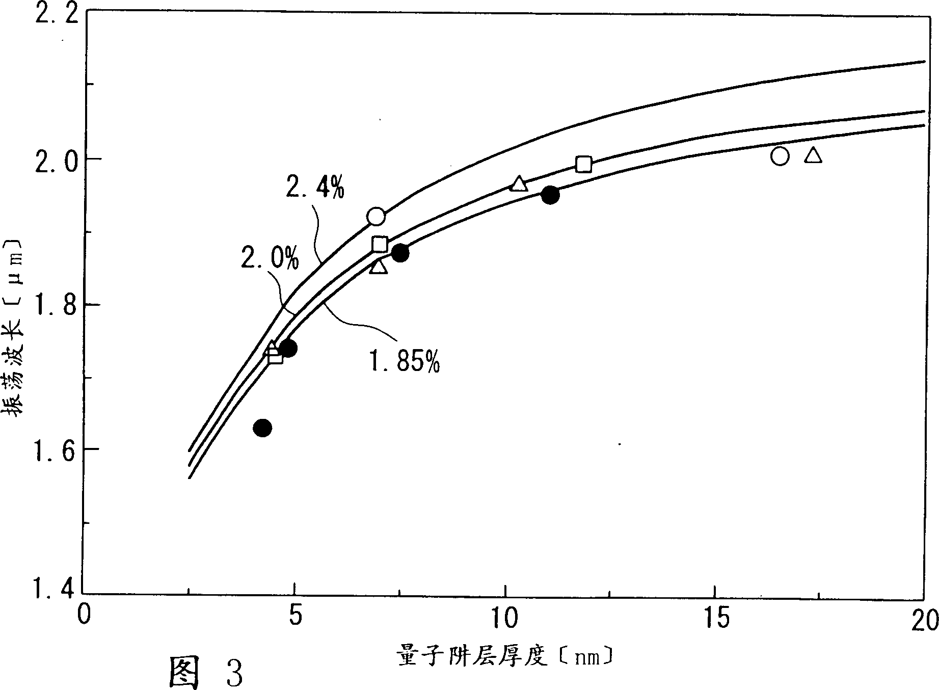
A semiconductor laser in the wavelength band of 1.3-1.55 mu m has been developed conventionally but a semiconductor laser in the wavelength band of 2 mu m, for which a wide field of technological application is expected, has not been developed sufficiently. A high-performance semiconductor laser oscillating in a wavelenght band of 2 mu m, specifically a compression strain quantum well semiconductor laser employing InGaAs / InGaAsP material oscillating in 2 mu m wavelength band, characterized in that the difference DELTA E between the band gap Eocl of an optical confinement layer and the emission transition energy Ewell between the ground levels of a quantum well layer is 275-300 meV.
Description
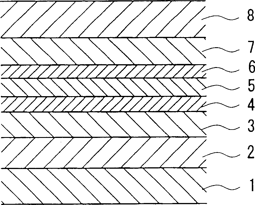
technical field [0001] The present invention relates to a compressive strain quantum well laser, and more specifically, relates to a semiconductor laser that uses InGaAs / InGaAsP materials and oscillates in a frequency band with a wavelength of 2 μm. [0002] This specification is based on a Japanese patent application (Japanese Patent Application No. Hei 9-252539), and the contents described in the Japanese application are incorporated as a part of this specification. Background technique [0003] InGaAs / InGaAsP materials are one of the most important materials for semiconductor lasers, especially InGaAs / InGaAsP series semiconductor lasers with quantum wells in the active layer have been practically used as light sources for communications in the 1.3μm to 1.55μm band . In the past, such quantum well active layers were formed using lattice matching. [0004] In recent years, it is desired to improve the various characteristics of the laser and to further improve the control...
Claims
Login to View More Application Information
Patent Timeline
 Patent Type & AuthorityPatents(China)
IPC IPC(8): H01S5/00H01S5/34H01S5/343
CPCH01S2302/00H01S5/3409H01S5/34306H01S5/34313B82Y20/00H01S5/30
Inventor董杰松本功
OwnerNIPPON SANSO CORP