Ge/gesn heterojunction laser and its preparation method

A laser and heterojunction technology, applied in lasers, laser parts, semiconductor lasers, etc., can solve the problems of many high-reflection coating layers, difficult process, easy to fall off, etc., to improve the limiting factor, simple process, Loss factor reduction effect

Active Publication Date: 2020-02-14
XIDIAN UNIV
View PDF6 Cites 0 Cited by
  • Summary
  • Abstract
  • Description
  • Claims
  • Application Information

AI Technical Summary

Problems solved by technology

[0008] 2. When the Fabry Perot resonator is used for the Ge-based laser, due to its large wavelength, the number of coating layers of the high-reflection film is also large, the process is difficult, and it is easy to fall off

Method used


Image

  • Ge/gesn heterojunction laser and its preparation method
  • Ge/gesn heterojunction laser and its preparation method
  • Ge/gesn heterojunction laser and its preparation method

Examples


Embodiment 1

[0048] In order to solve the problem that the luminous efficiency of the traditional Ge-based laser is not high, the threshold current density is relatively large, and its preparation process is difficult, this embodiment provides a method for preparing a Ge / GeSn heterojunction laser and the Ge / GeSn heterojunction laser prepared by this method. GeSn heterojunction lasers.

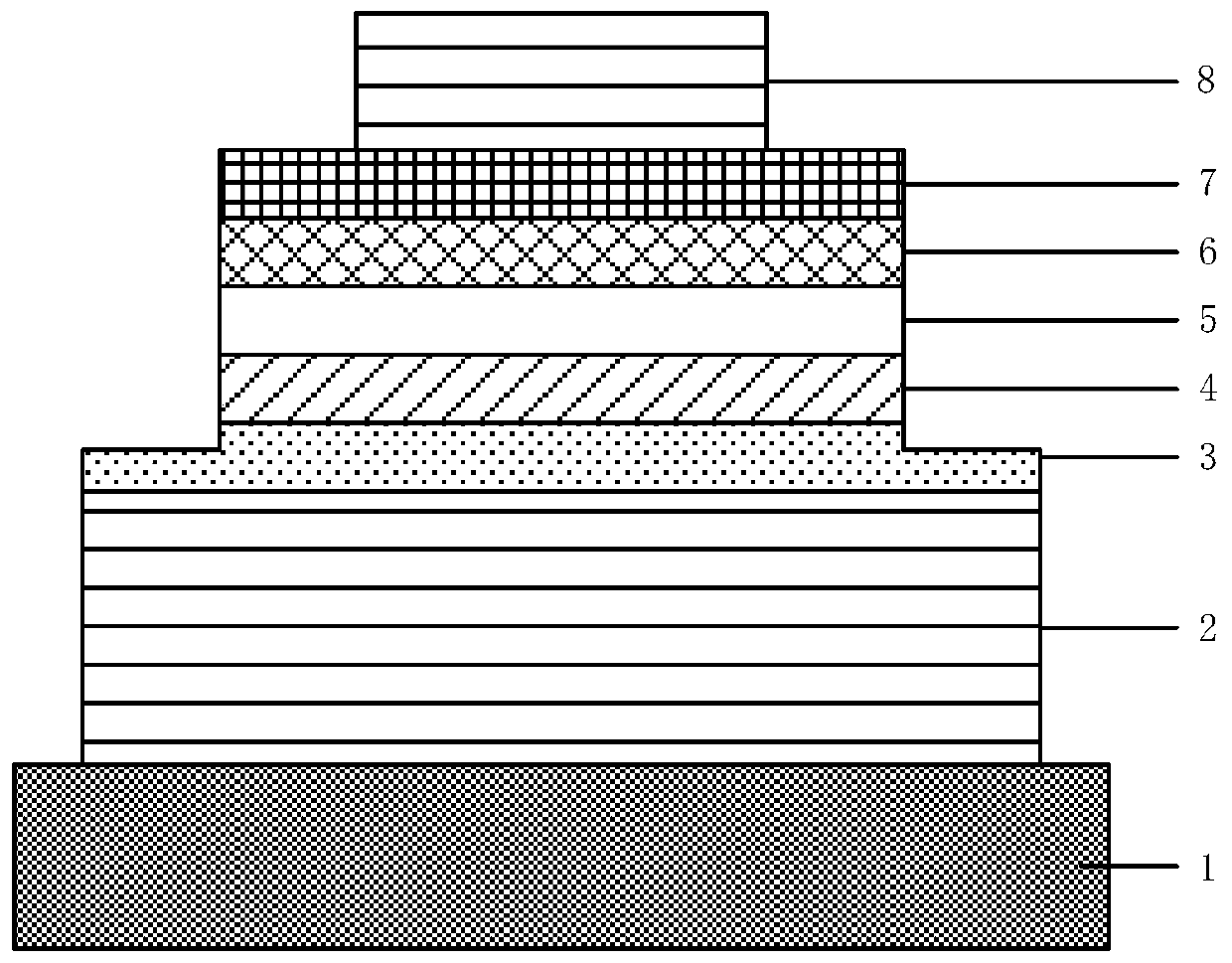
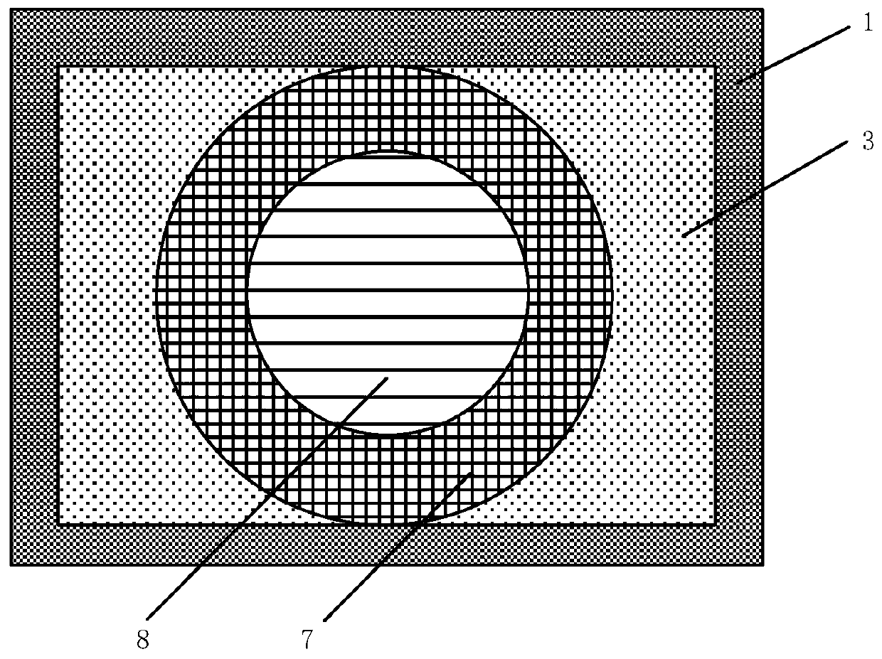
[0049] See figure 1 and figure 2 , figure 1 It is a schematic cross-sectional view of a Ge / GeSn heterojunction laser of the present invention, figure 2 It is a schematic top view of the Ge / GeSn heterojunction laser of the present invention. The Ge / GeSn heterojunction laser structure of the present invention is as follows from bottom to top: substrate 1, first Bragg mirror layer 2, first n-type Ge layer 3, second n-type Ge layer 4, GeSn layer 5, The first p-type Ge layer 6, the second p-type Ge layer 7, the second Bragg mirror layer 8; the second Bragg mirror layer 8 is columnar, the first n-type Ge la...

Embodiment 2

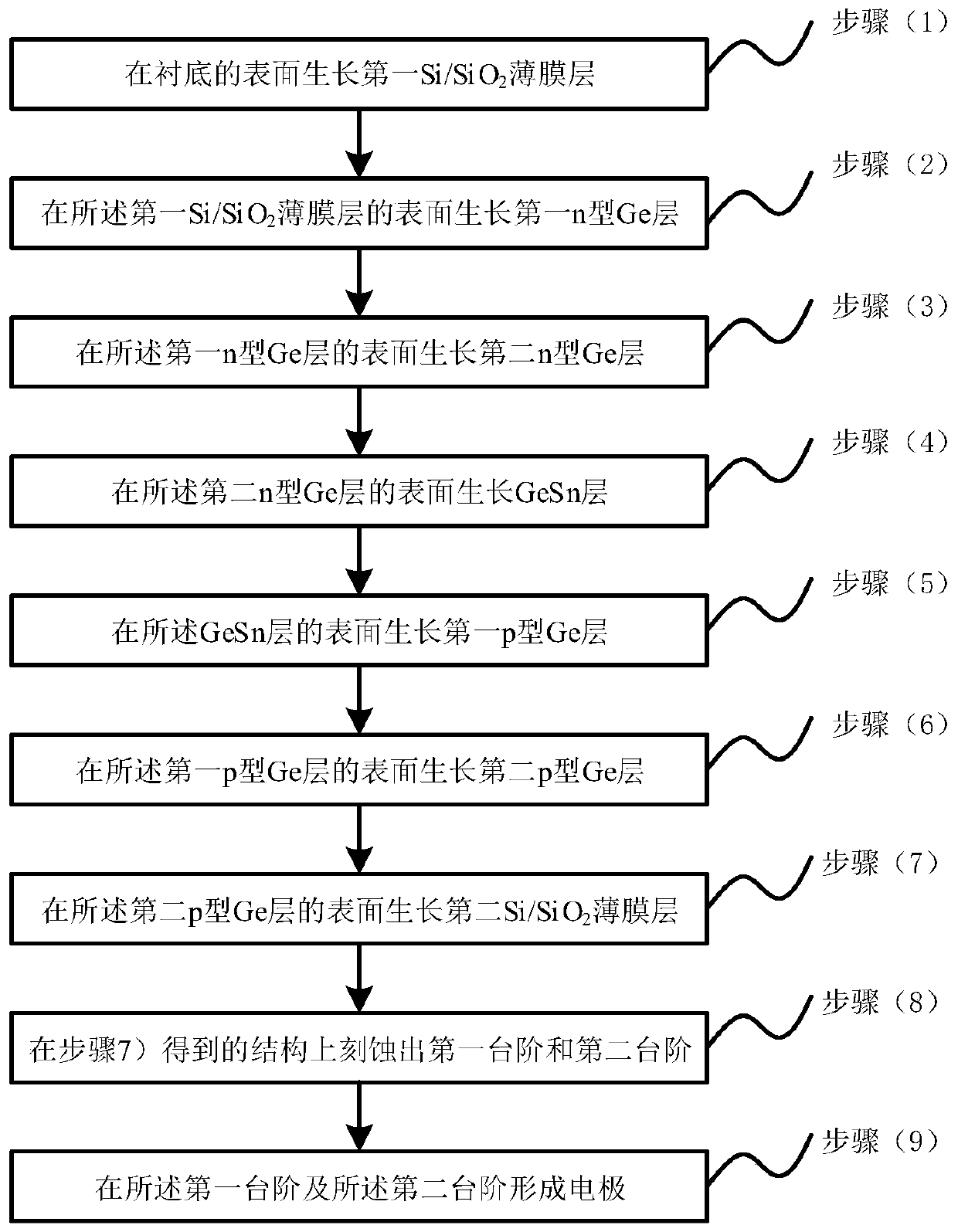
[0085] See 4(a) to 4(h), and figure 1 In this embodiment, on the basis of the above-mentioned embodiments, the preparation method of the Ge / GeSn heterojunction laser and the prepared Ge / GeSn heterojunction laser of the present invention are described in detail as follows:

[0086] Step (1), please refer to Fig. 4 (a), select the silicon material on the insulator or the bulk silicon material as the substrate, usually the substrate 1 is rectangular, and use plasma enhanced chemical vapor deposition (PECVD) to grow the first Si / SiO 2 film layer.

[0087] The switch of the mass flowmeter is controlled by the computer, so that the reaction gas in the reaction chamber alternates in the SiH 4 (+Ar) and O 2 Exchange between, so that the decomposition of SiH 4 Deposition of polysilicon film and pure oxygen layer-by-layer plasma oxidation are carried out alternately.

[0088] The substrate 1 temperature was kept at 250°C, Si and SiO 2 The thicknesses are 143nm and 233nm respectiv...


PUM

PropertyMeasurementUnit
current densityaaaaaaaaaa
radiusaaaaaaaaaa
heightaaaaaaaaaa

Abstract

The invention discloses a Ge / GeSn heterojunction laser and a preparation method thereof. The method includes: growing a first Bragg reflective mirror layer on the surface of a substrate; growing a first n-type Ge layer on the surface of the first Bragg mirror layer; growing a second n-type Ge layer on the surface of the first n-type Ge layer; growing a GeSn layer on the surface of the second n-type Ge layer; growing a first p-type Ge layer on the surface of the GeSn layer; growing a second p-type Ge layer on the surface of the first p-type Ge layer; growing a second Bragg mirror layer on the surface of the second p-type Ge layer; etching a first cylinder and a second cylinder on the obtained structure; forming an electrode at the first step and the second step; finally forming a Ge / GeSn heterojunction lase is finally formed. The invention adopts GeSn material instead of traditional single Ge material to improve luminescence efficiency; By using P-I-N structure reduces the threshold current density. In addition, the preparation method of the invention is simple in process.

Description

technical field [0001] The invention belongs to the technical field of semiconductors, and in particular relates to a Ge / GeSn heterojunction laser and a preparation method thereof. Background technique [0002] As we all know, large-scale integrated circuits on silicon chips show the powerful signal processing functions of electronics, and the global optical fiber communication network shows the superior transmission performance of photons. Silicon-based optoelectronic integration combines the two advantages of electronic signal processing function and photon transmission performance to achieve high-speed, low-energy, and interference-free chip optical interconnection. At present, most of the commercial optoelectronic devices use III-V semiconductor materials, and its process is not compatible with the large-scale integration process, and the technology of bonding wafers to silicon wafers is expensive and has low yield, resulting in the optoelectronics of III-V and chips. H...

Claims


Application Information

Patent Timeline
Patent Type & Authority Patents(China)
IPC IPC(8): H01S5/32H01S5/30H01S5/125
CPCH01S5/125H01S5/3027H01S5/3223
Inventor 舒斌张利锋高玉龙胡辉勇王斌王利明韩本光张鹤鸣
Owner XIDIAN UNIV
Why Eureka
Try Eureka