Reliability test system for laser chip

A test system and reliability technology, applied in the field of reliability test systems for laser chips, can solve problems such as troublesome and poor temperature control accuracy

Pending Publication Date: 2020-10-23
苏州联讯仪器股份有限公司
View PDF0 Cites 0 Cited by
  • Summary
  • Abstract
  • Description
  • Claims
  • Application Information

AI Technical Summary

Problems solved by technology

[0003] The burn-in test can be used as a device reliability test or as a production window to find early failures of the device. Generally, the device used for chip burn-in test is to work together with the external circuit board through the

Method used


Image

  • Reliability test system for laser chip
  • Reliability test system for laser chip
  • Reliability test system for laser chip

Examples


Embodiment 1

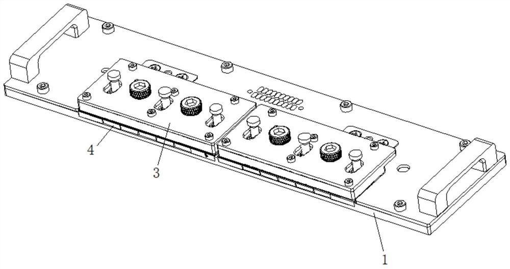
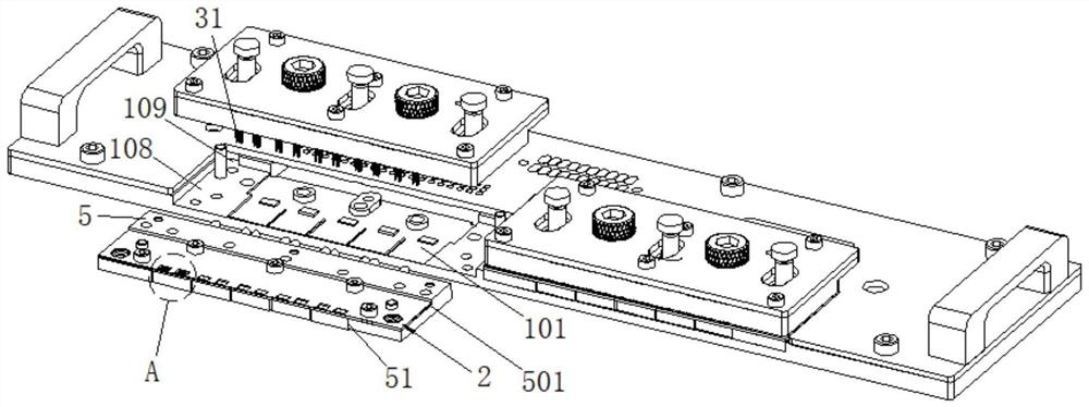
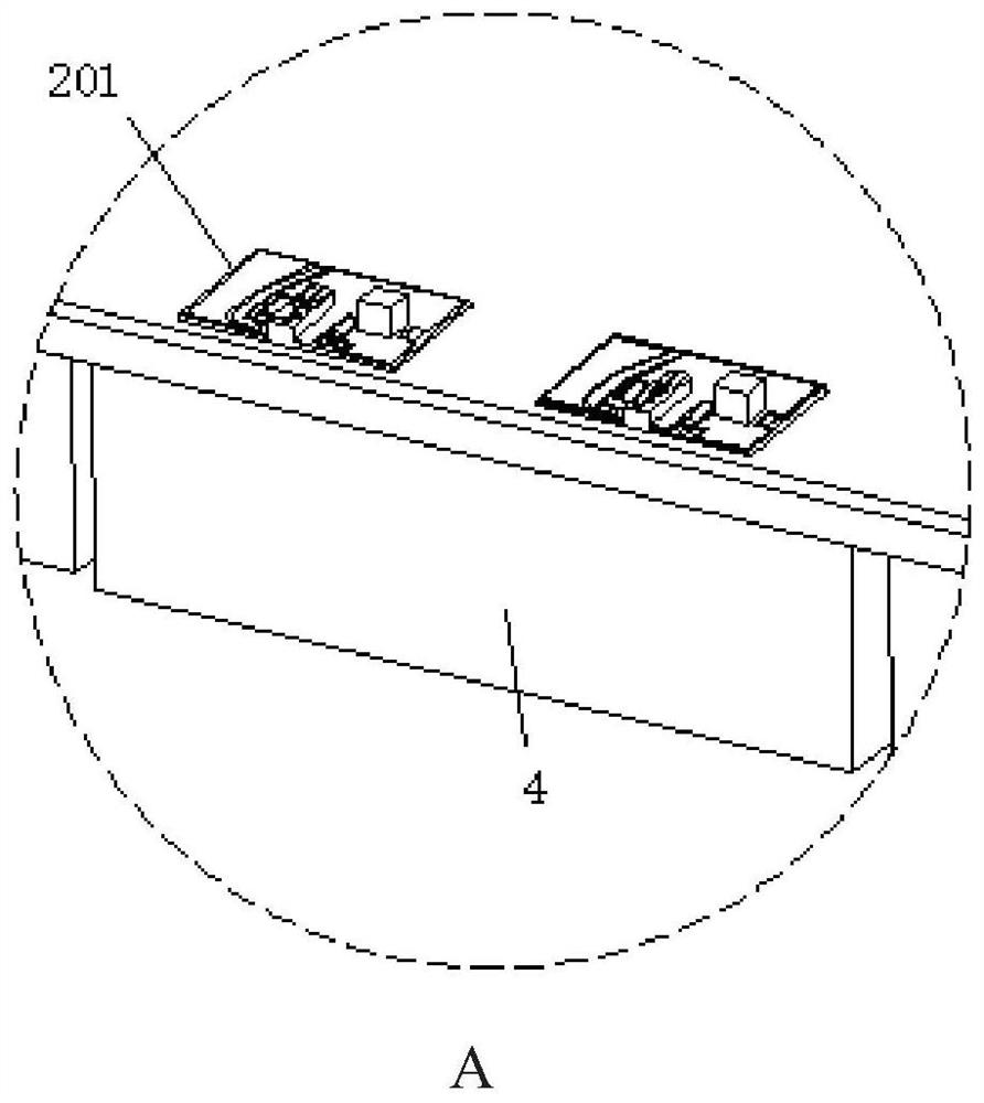
[0030] Embodiment 1: a kind of reliability test system for laser chips, with reference to the attached Figure 1-6 , including a substrate 1, a carrier 2 mounted on the substrate 1, and a first PCB3 mounted on the carrier 2, the carrier 2 has a chip slot 201 for chip embedding, and the first PCB3 has a The chip probe 31 corresponding to the chip slot 201, several TEC4s are installed between the substrate 1 and the carrier board 2, and the TEC4 is located directly below the chip slot 201, and a thermal insulation is installed between the substrate 1 and the first PCB3. A plate 5, which is provided with a heat-insulating groove 51 for TEC4 to be embedded in the heat-shielding plate 5;

[0031] The first PCB3 is installed on the heat shield 5, and a second PCB6 is installed on the substrate 1, and the second PCB6 has a connecting contact 61, a test contact 62 communicated with the connecting contact 61, a soldering contact 63 and the power supply contact 63 communicated with the...

Embodiment 2

[0037] Embodiment 2: a kind of reliability testing system for laser chips, with reference to the attached Figure 1-6 , including a substrate 1, a carrier 2 mounted on the substrate 1, and a first PCB3 mounted on the carrier 2, the carrier 2 has a chip slot 201 for chip embedding, and the first PCB3 has a The chip probe 31 corresponding to the chip slot 201, several TEC4s are installed between the substrate 1 and the carrier board 2, and the TEC4 is located directly below the chip slot 201, and a thermal insulation is installed between the substrate 1 and the first PCB3. A plate 5, which is provided with a heat-insulating groove 51 for TEC4 to be embedded in the heat-shielding plate 5;

[0038] The first PCB3 is installed on the heat shield 5, and a second PCB6 is installed on the substrate 1, and the second PCB6 has a connecting contact 61, a test contact 62 communicated with the connecting contact 61, a soldering contact 63 and the power supply contact 63 communicated with ...


PUM


Abstract

The invention discloses a reliability test system for a laser chip. The system comprises a substrate, a carrier plate, and a first PCB, wherein the carrier plate is provided with a chip groove, the first PCB is provided with a chip probe, a TEC is disposed between the substrate and the carrier plate, a thermal insulation plate is disposed between the substrate and the first PCB, and a thermal insulation through groove is disposed in the thermal insulation plate; a second PCB is provided with a connection contact, a test contact, a welding contact and a power supply contact; the first PCB and abase plate are installed on the substrate through a fixing screw; the substrate is also provided with a limiting rod; the limiting rod is sleeved with a limiting spring; the base plate is provided with a limiting hole allowing a limiting rod to be embedded therein; the portion, on one side of the limiting hole, of the base plate is also provided with a strip-shaped guide hole in a communicating mode, and the strip-shaped guide hole is located in the side, close to the chip, of the base plate; the welding contact is located on the bottom surface of the second PCB; and a welding through hole corresponding to the welding contact is formed in the bottom surface of the substrate. According to the invention, temperature control precision can be improved; and a plurality of chips can be tested at a time, so test efficiency is effectively improved.

Description

technical field [0001] The invention relates to a reliability testing system for laser chips, which belongs to the technical field of chip processing. Background technique [0002] Chip burn-in testing is an electrical stress testing method that uses voltage and high temperature to accelerate the electrical failure of a device, in which the burn-in process basically simulates running the entire life of the chip because the electrical stimulus applied during the burn-in process reflects the worst-case operation of the chip . [0003] The burn-in test can be used as a device reliability test or as a production window to find early failures of the device. Generally, the device used for chip burn-in test is to work together with the external circuit board through the test socket. In the existing burn-in test fixture, The heating source that provides the temperature is far away from the chip, the temperature control accuracy is poor, and only a single chip can be tested at a tim...

Claims


Application Information

Patent Timeline
IPC IPC(8): G01R31/28G01R1/04
CPCG01R1/0408G01R31/28
Inventor 徐鹏嵩罗跃浩赵山郭孝明王化发黄建军
Owner 苏州联讯仪器股份有限公司
Why Eureka
Try Eureka