Substrate for enhancing magneto-optical effect by applying silicon micro-nano structure
A technology of micro-nano structure and structural enhancement, applied in optics, optical components, nonlinear optics, etc., can solve the problems of weak surface plasmon effect and weak magneto-optic effect, achieve good application value, improve strength, enhance The effect of the magneto-optical effect
- Summary
- Abstract
- Description
- Claims
- Application Information
AI Technical Summary
Problems solved by technology
Method used
Image
Examples
Embodiment 1
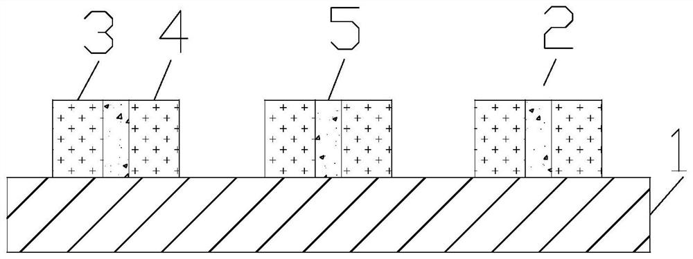
[0020] The invention provides a substrate for enhancing the magneto-optical effect by applying silicon microstructure. Such as figure 1 As shown, the substrate includes a base 1 and microstructure units 2 arranged periodically. The material of the base 1 is non-magnetic material. Preferably, the material of the substrate 1 is silicon dioxide. The microstructure unit 2 is in the shape of a one-dimensional wire grid. The microstructure units 2 are placed on the substrate 1 periodically. That is to say, the microstructure units 2 are a one-dimensional array. The microstructure unit 2 includes a first micro-nano structure part 3, a second micro-nano structure part 4, and a magnetic material part 5, and the first micro-nano structure part 3, the second micro-nano structure part 4, and the magnetic material part 5 are all placed on the substrate 1 on. That is to say, the first micro-nano structure part 3 , the second micro-nano structure part 4 and the magnetic material part 5...
Embodiment 2
[0026] On the basis of Example 1, the height of the first micro-nano structure part 3 and the second micro-nano structure part 4 is greater than 400 nanometers, and the distance between the first micro-nano structure part 3 and the second micro-nano structure part 4 is less than 50 nm. Nano. Furthermore, the height of the first micro-nano structure part 3 and the second micro-nano structure part 4 is greater than 500 nanometers, and the distance between the first micro-nano structure part 3 and the second micro-nano structure part 4 is less than 40 nanometers. In this way, a gap is formed between the first micro-nano structure part 3 and the second micro-nano structure part 4 . Under the action of excitation light, a strong electric field in the same direction is gathered in the gap, and the strong electric field has a stronger interaction with the magnetic material, thereby increasing the intensity of the magneto-optic effect.
Embodiment 3
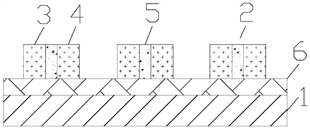
[0028] On the basis of embodiment 2, a thin film layer 6 is also included, and the thin film layer 6 is placed between the substrate 1 and the microstructure unit 2 . The material of the film layer 6 is noble metal. In this way, the film layer 6 reflects the electric field between the first micro-nano structure part 3 and the second micro-nano structure part 4, forming a stronger electric field concentration in the gap, further enhancing the interaction between the local electric field and the magnetic material, Enhance the magneto-optical effect.
[0029] Furthermore, a groove is provided on the top of the film layer 6 under the gap formed by the first micro-nano structure part 3 and the second micro-nano structure part 4 . The shape of the cross-section of the groove can be wedge-shaped, square or semi-circular. On the one hand, the grooves can be filled with magnetic materials, so that more magnetic materials can produce magneto-optic effects; on the other hand, under the...
PUM
 Abstract
Description
Claims
Application Information

