Array substrate, array substrate manufacturing method and display panel

An array substrate and bottom surface technology, applied in semiconductor/solid-state device manufacturing, electrical components, electric solid-state devices, etc., can solve the problem of small light emission range in the pixel area

Active Publication Date: 2020-10-30
WUHAN CHINA STAR OPTOELECTRONICS SEMICON DISPLAY TECH CO LTD
View PDF8 Cites 2 Cited by
  • Summary
  • Abstract
  • Description
  • Claims
  • Application Information

AI Technical Summary

Problems solved by technology

[0003] Embodiments of the present application provide an array substrate, an array substrate manufacturing method, and a display panel, which can improve the problem of a small light emission range in the pixel area

Method used


Image

  • Array substrate, array substrate manufacturing method and display panel
  • Array substrate, array substrate manufacturing method and display panel
  • Array substrate, array substrate manufacturing method and display panel

Examples


Embodiment Construction

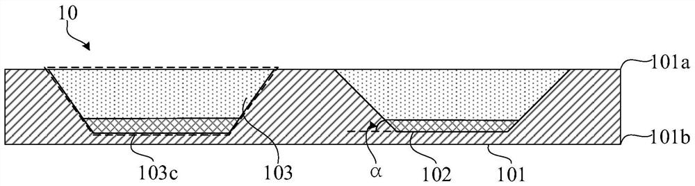
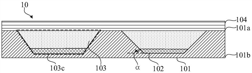
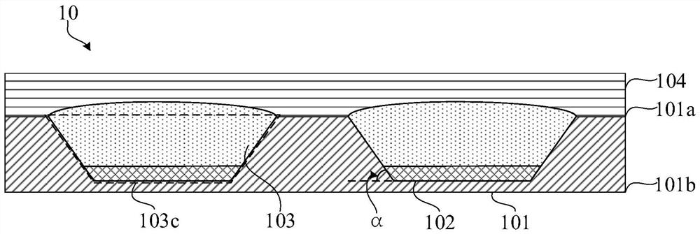
[0033] The technical solutions in the embodiments of the present application will be clearly and completely described below in conjunction with the drawings in the embodiments of the present application. Apparently, the described embodiments are only some of the embodiments of this application, not all of them. Based on the embodiments in this application, all other embodiments obtained by those skilled in the art without making creative efforts belong to the scope of protection of this application.

[0034] It should be noted that in the description of the present application, it should be understood that the terms "upper", "lower", "front", "rear", "left", "right", "inner", "outer", etc. The indicated orientation or positional relationship is based on the orientation or positional relationship shown in the drawings, and is only for the convenience of describing the present application and simplifying the description, rather than indicating or implying that the referred devic...


PUM

PropertyMeasurementUnit
diameteraaaaaaaaaa

Abstract

The embodiment of the invention provides an array substrate, an array substrate manufacturing method and a display panel. The array substrate comprises a pixel definition layer, a light-emitting layerand a transparent light guide layer. The pixel definition layer is provided with a first face and a second face which are oppositely arranged, a plurality of grooves are formed in the first face, andthe angle formed by the extension lines of the side face and the bottom face of the groove ranges from 0 degree to 50 degrees. The light-emitting layer is arranged on the bottom surface of the groove. The transparent light guide layer is filled in the groove and is positioned at the side, far away from the bottom surface of the groove, of the light-emitting layer. The groove is filled with the transparent light guide layer, and after light of the light-emitting layer is refracted by the transparent light guide layer, the emergence angle of the light can be increased. In addition, after the groove is filled with the transparent light guide layer, the problem that the bottom of the groove has an angle and is difficult to package can be solved. After the transparent light guide layer is filled, the leveling performance of material during ink-jet printing can be improved, and a thinning effect is brought to ink-jet printing.

Description

technical field [0001] The present application relates to the field of display technology, in particular to an array substrate, a manufacturing method of the array substrate, and a display panel. Background technique [0002] The current mainstream organic electroluminescent display device (Organic Light-Emitting Diode, OLED) evaporation and packaging process is to evaporate the corresponding organic light-emitting diodes in the pixel area divided by the pixel definition layer (PDL) produced by the array process. Luminescent materials are then packaged and protected by physical vapor deposition (Physical Vapor Deposition, PVD), chemical vapor deposition (Chemical Vapor Deposition, CVD) and ink jet printing (ink jet print, IJP) and other processes. In order to prevent color mixing due to the diffusion of evaporated materials, the pixel area is often designed as a pit structure, and organic light-emitting materials are generally evaporated at the bottom of the corresponding pi...

Claims


Application Information

Patent Timeline
Patent Type & Authority Applications(China)
IPC IPC(8): H01L51/52H01L51/56H01L27/32
CPCH10K59/122H10K59/12H10K50/858H10K59/1201H10K71/00
Inventor 齐晓青
Owner WUHAN CHINA STAR OPTOELECTRONICS SEMICON DISPLAY TECH CO LTD
Why Eureka
Try Eureka